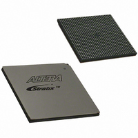
EP1S40B956C5 Altera, EP1S40B956C5 Datasheet - Page 411

EP1S40B956C5
Manufacturer Part Number
EP1S40B956C5
Description
IC STRATIX FPGA 40K LE 956-BGA
Manufacturer
Altera
Series
Stratix®r
Datasheet
1.EP1S10F484I6N.pdf
(864 pages)
Specifications of EP1S40B956C5
Number Of Logic Elements/cells
41250
Number Of Labs/clbs
4125
Total Ram Bits
3423744
Number Of I /o
683
Voltage - Supply
1.425 V ~ 1.575 V
Mounting Type
Surface Mount
Operating Temperature
0°C ~ 85°C
Package / Case
956-BGA
Lead Free Status / RoHS Status
Contains lead / RoHS non-compliant
Number Of Gates
-
Available stocks
Company
Part Number
Manufacturer
Quantity
Price
Part Number:
EP1S40B956C5
Manufacturer:
ALTERA/阿尔特拉
Quantity:
20 000
- Current page: 411 of 864
- Download datasheet (11Mb)
Altera Corporation
June 2006
Command & Address Pins
You can use any of the user I/O pins in the top or bottom bank of the
device (I/O banks 3, 4, 7, or 8) for commands and addresses. For DDR
SDRAM, you can also use any of the user I/O pins in the side I/O banks
1, 2, 5, or 6, regardless of whether you use the DQS phase-shift circuitry
or not.
Other Pins (Parity, DM, ECC & QVLD Pins)
You can use any of the DQ pins for the parity pins in Stratix and
Stratix GX devices. However, this may mean that you are using the next
larger DQS/DQ mode. For example, if you need a parity bit for each byte
of data, you are actually going to have nine DQ pins per DQS pin. The
Quartus II software then implements a ×16 mode, with the seven unused
DQ pins available as user I/O pins.
The data mask (DM) pins are only required when writing to
DDR SDRAM and RLDRAM II devices. A low signal on the DM pins
indicates that the write is valid. If the DM signal is high, the memory
masks the DQ signals. You can use any of the I/O pins in the same bank
as the DQ pins for the DM signals. Each group of DQS and DQ signals
requires a DM pin. The DDR register, clocked by the –90° shifted clock,
creates the DM signals, similar to DQ output signals.
Some DDR SDRAM devices support error correction coding (ECC),
which is a method of detecting and automatically correcting errors in
data transmission. Connect the DDR ECC pins to a Stratix and Stratix GX
device DQS/DQ group. In 72-bit DDR SDRAM, there are eight ECC pins
in addition to the 64 data pins. The memory controller needs extra logic
to encode and decode the ECC data.
QVLD pins are used in RLDRAM II interfacing to indicate the read data
availability. There is one QVLD pin per RLDRAM II device. A high on
QVLD indicates that the memory is outputting the data requested.
Similar to DQ inputs, this signal is edge-aligned with the RLDRAM II
read clocks, QK and QK#, and is sent half a clock cycle before data starts
coming out of the memory. You can connect QVLD pins to any of the I/O
pins in the same bank as the DQ pins for the QVLD signals.
DQS Phase-Shift Circuitry
Two single phase-shifting reference circuits are located on the top and
bottom of the Stratix and Stratix GX devices. Each circuit is driven by a
system reference clock that is of the same frequency as the DQS signal.
Clock pins CLK[15..12]p feed the phase-shift circuitry on the top of the
device and clock pins CLK[7..4]p feed the phase-shift circuitry on the
External Memory Interfaces in Stratix & Stratix GX Devices
Stratix Device Handbook, Volume 2
3–15
Related parts for EP1S40B956C5
Image
Part Number
Description
Manufacturer
Datasheet
Request
R

Part Number:
Description:
CYCLONE II STARTER KIT EP2C20N
Manufacturer:
Altera
Datasheet:

Part Number:
Description:
CPLD, EP610 Family, ECMOS Process, 300 Gates, 16 Macro Cells, 16 Reg., 16 User I/Os, 5V Supply, 35 Speed Grade, 24DIP
Manufacturer:
Altera Corporation
Datasheet:

Part Number:
Description:
CPLD, EP610 Family, ECMOS Process, 300 Gates, 16 Macro Cells, 16 Reg., 16 User I/Os, 5V Supply, 15 Speed Grade, 24DIP
Manufacturer:
Altera Corporation
Datasheet:

Part Number:
Description:
Manufacturer:
Altera Corporation
Datasheet:

Part Number:
Description:
CPLD, EP610 Family, ECMOS Process, 300 Gates, 16 Macro Cells, 16 Reg., 16 User I/Os, 5V Supply, 30 Speed Grade, 24DIP
Manufacturer:
Altera Corporation
Datasheet:

Part Number:
Description:
High-performance, low-power erasable programmable logic devices with 8 macrocells, 10ns
Manufacturer:
Altera Corporation
Datasheet:

Part Number:
Description:
High-performance, low-power erasable programmable logic devices with 8 macrocells, 7ns
Manufacturer:
Altera Corporation
Datasheet:

Part Number:
Description:
Classic EPLD
Manufacturer:
Altera Corporation
Datasheet:

Part Number:
Description:
High-performance, low-power erasable programmable logic devices with 8 macrocells, 10ns
Manufacturer:
Altera Corporation
Datasheet:

Part Number:
Description:
Manufacturer:
Altera Corporation
Datasheet:

Part Number:
Description:
Manufacturer:
Altera Corporation
Datasheet:

Part Number:
Description:
Manufacturer:
Altera Corporation
Datasheet:

Part Number:
Description:
CPLD, EP610 Family, ECMOS Process, 300 Gates, 16 Macro Cells, 16 Reg., 16 User I/Os, 5V Supply, 25 Speed Grade, 24DIP
Manufacturer:
Altera Corporation
Datasheet:


