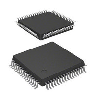
DF71251AD50FPV Renesas Electronics America, DF71251AD50FPV Datasheet - Page 773

DF71251AD50FPV
Manufacturer Part Number
DF71251AD50FPV
Description
MCU RISC FLASH 32K 8K 64LQFP
Manufacturer
Renesas Electronics America
Series
SuperH® SH Tinyr
Datasheet
1.DF71243N50FPV.pdf
(794 pages)
Specifications of DF71251AD50FPV
Core Processor
SH-2
Core Size
32-Bit
Speed
50MHz
Connectivity
SCI
Peripherals
POR, PWM, WDT
Number Of I /o
37
Program Memory Size
32KB (32K x 8)
Program Memory Type
FLASH
Ram Size
8K x 8
Voltage - Supply (vcc/vdd)
4 V ~ 5.5 V
Data Converters
A/D 8x10b
Oscillator Type
External
Operating Temperature
-40°C ~ 85°C
Package / Case
64-LQFP
Lead Free Status / RoHS Status
Lead free / RoHS Compliant
Eeprom Size
-
Available stocks
Company
Part Number
Manufacturer
Quantity
Price
Company:
Part Number:
DF71251AD50FPV
Manufacturer:
Renesas Electronics America
Quantity:
10 000
- Current page: 773 of 794
- Download datasheet (5Mb)
Item
12.3.8 Serial Port Register
(SCSPTR)
12.4.5 Multiprocessor Serial
Data Transmission
Figure 12.16 Sample
Multiprocessor Serial
Transmission Flowchart
Page Revision (See Manual for Details)
430
467
Figure amended
Table amended
Figure amended
Initial value:
Bit
2
Write transmit data to SCTDR and
as an output port with the PFC
Clear TE bit in SCSCR to 0;
Read TDRE flag in SCSSR
Read TEND flag in SCSSR
set MPBT bit in SCSSR
Clear TDRE flag to 0
All data transmitted?
Clear SPBODT to 0
R/W:
select the TXD pin
Start transmission
Bit Name
SPB1DT
Bit:
Break output?
Initialization
TDRE = 1?
TEND = 1?
<End>
R/W
EIO
Yes
Yes
Yes
Yes
7
0
Initial
value
Undefined W
6
0
-
-
Rev. 5.00 Mar. 06, 2009 Page 753 of 770
R/W
No
No
No
No
5
0
-
-
Description
Clock Port Data in Serial Port
Specifies the data output through the SCK pin in the
serial port. Output should be enabled by the SPB1IO bit
(for details, refer to the SPB1IO bit description). When
output is enabled, the SPB1DT bit value is output
through the SCK pin.
0: Low level is output
1: High level is output
[1]
[2]
[3]
[4]
4
0
-
-
[1]
[2]
[3]
[4]
SPB1IO SPB1DT
R/W
3
0
SCI initialization:
Set the TXD pin using the PFC.
After the TE bit is set to 1, 1 is output
for one frame, and transmission is
enabled. However, data is not
transmitted.
SCI status check and transmit data
write:
Read SCSSR and check that the
TDRE flag is set to 1, then write
transmit data to SCTDR. Set the
MPBT bit in SCSSR to 0 or 1. Finally,
clear the TDRE flag to 0.
After initializing the SCI, when an ID
is written to SCTDR register so as to
transmit the ID, data is immediately
transferred, and then the TDER flag is
set to 1. The MPBT bit must be held 1
because the ID is not transmitted from
the TXD pin at this time. When the
TDRE flag is set to 1 after data
following the ID is written to SCTDR,
clear the MPBT bit to 0.
Serial transmission continuation
procedure:
To continue serial transmission, be
sure to read 1 from the TDRE flag to
confirm that writing is possible, then
write data to SCTDR, and then clear
the TDRE flag to 0.
Break output at the end of serial
transmission:
To output a break during serial
transmission, first clear the SPBODT
bit in the serial port register
(SCSPTR) to 0, then clear the TE bit
in SCSCR to 0 and use the PFC to
select the TXD pin as an output port.
Undefined
REJ09B0243-0500
W
2
1
0
-
-
SPB0DT
W
0
1
Related parts for DF71251AD50FPV
Image
Part Number
Description
Manufacturer
Datasheet
Request
R

Part Number:
Description:
KIT STARTER FOR M16C/29
Manufacturer:
Renesas Electronics America
Datasheet:

Part Number:
Description:
KIT STARTER FOR R8C/2D
Manufacturer:
Renesas Electronics America
Datasheet:

Part Number:
Description:
R0K33062P STARTER KIT
Manufacturer:
Renesas Electronics America
Datasheet:

Part Number:
Description:
KIT STARTER FOR R8C/23 E8A
Manufacturer:
Renesas Electronics America
Datasheet:

Part Number:
Description:
KIT STARTER FOR R8C/25
Manufacturer:
Renesas Electronics America
Datasheet:

Part Number:
Description:
KIT STARTER H8S2456 SHARPE DSPLY
Manufacturer:
Renesas Electronics America
Datasheet:

Part Number:
Description:
KIT STARTER FOR R8C38C
Manufacturer:
Renesas Electronics America
Datasheet:

Part Number:
Description:
KIT STARTER FOR R8C35C
Manufacturer:
Renesas Electronics America
Datasheet:

Part Number:
Description:
KIT STARTER FOR R8CL3AC+LCD APPS
Manufacturer:
Renesas Electronics America
Datasheet:

Part Number:
Description:
KIT STARTER FOR RX610
Manufacturer:
Renesas Electronics America
Datasheet:

Part Number:
Description:
KIT STARTER FOR R32C/118
Manufacturer:
Renesas Electronics America
Datasheet:

Part Number:
Description:
KIT DEV RSK-R8C/26-29
Manufacturer:
Renesas Electronics America
Datasheet:

Part Number:
Description:
KIT STARTER FOR SH7124
Manufacturer:
Renesas Electronics America
Datasheet:

Part Number:
Description:
KIT STARTER FOR H8SX/1622
Manufacturer:
Renesas Electronics America
Datasheet:

Part Number:
Description:
KIT DEV FOR SH7203
Manufacturer:
Renesas Electronics America
Datasheet:


