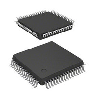
DF71251AD50FPV Renesas Electronics America, DF71251AD50FPV Datasheet - Page 44

DF71251AD50FPV
Manufacturer Part Number
DF71251AD50FPV
Description
MCU RISC FLASH 32K 8K 64LQFP
Manufacturer
Renesas Electronics America
Series
SuperH® SH Tinyr
Datasheet
1.DF71243N50FPV.pdf
(794 pages)
Specifications of DF71251AD50FPV
Core Processor
SH-2
Core Size
32-Bit
Speed
50MHz
Connectivity
SCI
Peripherals
POR, PWM, WDT
Number Of I /o
37
Program Memory Size
32KB (32K x 8)
Program Memory Type
FLASH
Ram Size
8K x 8
Voltage - Supply (vcc/vdd)
4 V ~ 5.5 V
Data Converters
A/D 8x10b
Oscillator Type
External
Operating Temperature
-40°C ~ 85°C
Package / Case
64-LQFP
Lead Free Status / RoHS Status
Lead free / RoHS Compliant
Eeprom Size
-
Available stocks
Company
Part Number
Manufacturer
Quantity
Price
Company:
Part Number:
DF71251AD50FPV
Manufacturer:
Renesas Electronics America
Quantity:
10 000
- Current page: 44 of 794
- Download datasheet (5Mb)
Load/Store Architecture: Basic operations are executed between registers. In operations
involving memory, data is first loaded into a register (load/store architecture). However, bit
manipulation instructions such as AND are executed directly in memory.
Delayed Branching: Unconditional branch instructions means the delayed branch instructions.
With a delayed branch instruction, the branch is made after execution of the instruction
immediately following the delayed branch instruction. This minimizes disruption of the pipeline
when a branch is made. The conditional branch instructions have two types of instructions:
conditional branch instructions and delayed branch instructions.
Table 2.3
Multiply/Multiply-and-Accumulate Operations: A 16 × 16 → 32 multiply operation is
executed in one to two cycles, and a 16 × 16 + 64 → 64 multiply-and-accumulate operation in two
to three cycles. A 32 × 32 → 64 multiply operation and a 32 × 32 + 64 → 64 multiply-and-
accumulate operation are each executed in two to four cycles.
T Bit: The result of a comparison is indicated by the T bit in SR, and a conditional branch is
performed according to whether the result is True or False. Processing speed has been improved
by keeping the number of instructions that modify the T bit to a minimum.
Table 2.4
Immediate Data: 8-bit immediate data is placed in the instruction code. Word and longword
immediate data is not placed in the instruction code. It is placed in a table in memory. The table in
memory is accessed with the MOV immediate data instruction using PC relative addressing mode
with displacement.
Rev. 5.00 Mar. 06, 2009 Page 24 of 770
REJ09B0243-0500
CPU in this LSI
BRA
ADD
CPU in this LSI
CMP/GE
BT
BF
ADD
CMP/EQ
BT
TRGET
R1,R0
R1,R0
TRGET0
TRGET1
# 1 ,R0
#0,R0
TRGET
Delayed Branch Instructions
T Bit
Description
ADD is executed before branch to TRGET.
Description
When R0 ≥ R1, the T bit is set.
When R0 ≥ R1, a branch is made to TRGET0. BGE
When R0 < R1, a branch is made to TRGET1. BLT
The T bit is not changed by ADD.
When R0 = 0, the T bit is set.
A branch is made when R0 = 0.
Example of Other CPUs
ADD.W R1,R0
BRA
Example of Other CPUs
CMP.W R1,R0
SUB.W #1,R0
BEQ
TRGET0
TRGET1
TRGET
TRGET
Related parts for DF71251AD50FPV
Image
Part Number
Description
Manufacturer
Datasheet
Request
R

Part Number:
Description:
KIT STARTER FOR M16C/29
Manufacturer:
Renesas Electronics America
Datasheet:

Part Number:
Description:
KIT STARTER FOR R8C/2D
Manufacturer:
Renesas Electronics America
Datasheet:

Part Number:
Description:
R0K33062P STARTER KIT
Manufacturer:
Renesas Electronics America
Datasheet:

Part Number:
Description:
KIT STARTER FOR R8C/23 E8A
Manufacturer:
Renesas Electronics America
Datasheet:

Part Number:
Description:
KIT STARTER FOR R8C/25
Manufacturer:
Renesas Electronics America
Datasheet:

Part Number:
Description:
KIT STARTER H8S2456 SHARPE DSPLY
Manufacturer:
Renesas Electronics America
Datasheet:

Part Number:
Description:
KIT STARTER FOR R8C38C
Manufacturer:
Renesas Electronics America
Datasheet:

Part Number:
Description:
KIT STARTER FOR R8C35C
Manufacturer:
Renesas Electronics America
Datasheet:

Part Number:
Description:
KIT STARTER FOR R8CL3AC+LCD APPS
Manufacturer:
Renesas Electronics America
Datasheet:

Part Number:
Description:
KIT STARTER FOR RX610
Manufacturer:
Renesas Electronics America
Datasheet:

Part Number:
Description:
KIT STARTER FOR R32C/118
Manufacturer:
Renesas Electronics America
Datasheet:

Part Number:
Description:
KIT DEV RSK-R8C/26-29
Manufacturer:
Renesas Electronics America
Datasheet:

Part Number:
Description:
KIT STARTER FOR SH7124
Manufacturer:
Renesas Electronics America
Datasheet:

Part Number:
Description:
KIT STARTER FOR H8SX/1622
Manufacturer:
Renesas Electronics America
Datasheet:

Part Number:
Description:
KIT DEV FOR SH7203
Manufacturer:
Renesas Electronics America
Datasheet:


