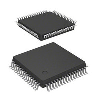
DF71251AD50FPV Renesas Electronics America, DF71251AD50FPV Datasheet - Page 238

DF71251AD50FPV
Manufacturer Part Number
DF71251AD50FPV
Description
MCU RISC FLASH 32K 8K 64LQFP
Manufacturer
Renesas Electronics America
Series
SuperH® SH Tinyr
Datasheet
1.DF71243N50FPV.pdf
(794 pages)
Specifications of DF71251AD50FPV
Core Processor
SH-2
Core Size
32-Bit
Speed
50MHz
Connectivity
SCI
Peripherals
POR, PWM, WDT
Number Of I /o
37
Program Memory Size
32KB (32K x 8)
Program Memory Type
FLASH
Ram Size
8K x 8
Voltage - Supply (vcc/vdd)
4 V ~ 5.5 V
Data Converters
A/D 8x10b
Oscillator Type
External
Operating Temperature
-40°C ~ 85°C
Package / Case
64-LQFP
Lead Free Status / RoHS Status
Lead free / RoHS Compliant
Eeprom Size
-
Available stocks
Company
Part Number
Manufacturer
Quantity
Price
Company:
Part Number:
DF71251AD50FPV
Manufacturer:
Renesas Electronics America
Quantity:
10 000
- Current page: 238 of 794
- Download datasheet (5Mb)
Note:
9.3.18
TOCR1 is an 8-bit readable/writable register that enables/disables PWM synchronized toggle
output in complementary PWM mode/reset synchronized PWM mode, and controls output level
inversion of PWM output.
Rev. 5.00 Mar. 06, 2009 Page 218 of 770
REJ09B0243-0500
Bit
0
Bit
7
6
5, 4
Note:
* The inactive level is determined by the settings in timer output control registers 1 and 2
Bit Name
OE3B
Bit Name
—
PSYE
—
Timer Output Control Register 1 (TOCR1)
*
(TOCR1 and TOCR2). For details, refer to section 9.3.18, Timer Output Control
Register 1 (TOCR1), and section 9.3.19, Timer Output Control Register 2 (TOCR2). Set
these bits to 1 to enable MTU2 output in other than complementary PWM or reset-
synchronized PWM mode. When these bits are set to 0, low level is output.
This bit can be set to 1 only once after a power-on reset. After 1 is written, 0 cannot be written to the bit.
Initial value:
Initial
Value
0
Initial
value
0
0
All 0
R/W:
Bit:
R
7
0
R/W
R/W
-
R/W
R
R/W
R
PSYE
R/W
6
0
Description
Master Enable TIOC3B
This bit enables/disables the TIOC3B pin MTU2 output.
0: MTU2 output is disabled (inactive level)*
1: MTU2 output is enabled
Description
Reserved
This bit is always read as 0. The write value should
always be 0.
This bit selects the enable/disable of toggle output
synchronized with the PWM period.
0: Toggle output is disabled
1: Toggle output is enabled
These bits are always read as 0. The write value should
always be 0.
PWM Synchronous Output Enable
Reserved
R
5
0
-
R
4
0
-
R/(W)* R/W
TOCL
3
0
TOCS
2
0
OLSN
R/W
1
0
OLSP
R/W
0
0
Related parts for DF71251AD50FPV
Image
Part Number
Description
Manufacturer
Datasheet
Request
R

Part Number:
Description:
KIT STARTER FOR M16C/29
Manufacturer:
Renesas Electronics America
Datasheet:

Part Number:
Description:
KIT STARTER FOR R8C/2D
Manufacturer:
Renesas Electronics America
Datasheet:

Part Number:
Description:
R0K33062P STARTER KIT
Manufacturer:
Renesas Electronics America
Datasheet:

Part Number:
Description:
KIT STARTER FOR R8C/23 E8A
Manufacturer:
Renesas Electronics America
Datasheet:

Part Number:
Description:
KIT STARTER FOR R8C/25
Manufacturer:
Renesas Electronics America
Datasheet:

Part Number:
Description:
KIT STARTER H8S2456 SHARPE DSPLY
Manufacturer:
Renesas Electronics America
Datasheet:

Part Number:
Description:
KIT STARTER FOR R8C38C
Manufacturer:
Renesas Electronics America
Datasheet:

Part Number:
Description:
KIT STARTER FOR R8C35C
Manufacturer:
Renesas Electronics America
Datasheet:

Part Number:
Description:
KIT STARTER FOR R8CL3AC+LCD APPS
Manufacturer:
Renesas Electronics America
Datasheet:

Part Number:
Description:
KIT STARTER FOR RX610
Manufacturer:
Renesas Electronics America
Datasheet:

Part Number:
Description:
KIT STARTER FOR R32C/118
Manufacturer:
Renesas Electronics America
Datasheet:

Part Number:
Description:
KIT DEV RSK-R8C/26-29
Manufacturer:
Renesas Electronics America
Datasheet:

Part Number:
Description:
KIT STARTER FOR SH7124
Manufacturer:
Renesas Electronics America
Datasheet:

Part Number:
Description:
KIT STARTER FOR H8SX/1622
Manufacturer:
Renesas Electronics America
Datasheet:

Part Number:
Description:
KIT DEV FOR SH7203
Manufacturer:
Renesas Electronics America
Datasheet:


