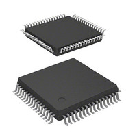
DF71251AD50FPV Renesas Electronics America, DF71251AD50FPV Datasheet - Page 287

DF71251AD50FPV
Manufacturer Part Number
DF71251AD50FPV
Description
MCU RISC FLASH 32K 8K 64LQFP
Manufacturer
Renesas Electronics America
Series
SuperH® SH Tinyr
Datasheet
1.DF71243N50FPV.pdf
(794 pages)
Specifications of DF71251AD50FPV
Core Processor
SH-2
Core Size
32-Bit
Speed
50MHz
Connectivity
SCI
Peripherals
POR, PWM, WDT
Number Of I /o
37
Program Memory Size
32KB (32K x 8)
Program Memory Type
FLASH
Ram Size
8K x 8
Voltage - Supply (vcc/vdd)
4 V ~ 5.5 V
Data Converters
A/D 8x10b
Oscillator Type
External
Operating Temperature
-40°C ~ 85°C
Package / Case
64-LQFP
Lead Free Status / RoHS Status
Lead free / RoHS Compliant
Eeprom Size
-
Available stocks
Company
Part Number
Manufacturer
Quantity
Price
Company:
Part Number:
DF71251AD50FPV
Manufacturer:
Renesas Electronics America
Quantity:
10 000
- Current page: 287 of 794
- Download datasheet (5Mb)
Procedure for Selecting the Reset-Synchronized PWM Mode: Figure 9.35 shows an example
of procedure for selecting the reset synchronized PWM mode.
Reset-synchronized PWM mode
PWM cycle output enabling,
Figure 9.35 Procedure for Selecting Reset-Synchronized PWM Mode
PWM output level setting
Select counter clock and
Enable waveform output
Set reset-synchronized
Start count operation
Brushless DC motor
counter clear source
Reset-synchronized
Stop counting
control setting
PWM mode
PFC setting
PWM mode
Set TCNT
Set TGR
Note: The output waveform starts to toggle operation at the point of
[1]
[2]
[3]
[4]
[5]
[6]
[7]
[8]
[9]
[10]
TCNT_3 = TGRA_3 = X by setting X = TGRA, i.e., cycle = duty.
[1] Clear the CST3 and CST4 bits in the TSTR
[2] Set bits TPSC2 to TPSC0 and CKEG1 and
[3] When performing brushless DC motor control,
[4] Reset TCNT_3 and TCNT_4 to H'0000.
[5] TGRA_3 is the period register. Set the waveform
[6] Select enabling/disabling of toggle output
[7] Set bits MD3 to MD0 in TMDR_3 to B'1000 to select
[8] Set the enabling/disabling of the PWM waveform output
[9] Set the port control register and the port I/O register.
[10] Set the CST3 bit in the TSTR to 1 to start the count
to 0 to halt the counting of TCNT. The
reset-synchronized PWM mode must be set
up while TCNT_3 and TCNT_4 are halted.
CKEG0 in the TCR_3 to select the counter
clock and clock edge for channel 3. Set bits
CCLR2 to CCLR0 in the TCR_3 to select TGRA
compare-match as a counter clear source.
set bit BDC in the timer gate control register
(TGCR) and set the feedback signal input source
and output chopping or gate signal direct output.
period value in TGRA_3. Set the transition timing
of the PWM output waveforms in TGRB_3,
TGRA_4, and TGRB_4. Set times within the
compare-match range of TCNT_3.
synchronized with the PMW cycle using bit PSYE
in the timer output control register (TOCR1), and set
the PWM output level with bits OLSP and OLSN.
When specifying the PWM output level by using TOLBR
as a buffer for TOCR2, see figure 9.3.
the reset-synchronized PWM mode. Do not set to TMDR_4.
pin in TOER.
operation.
X ≤ TGRA_3 (X: set value).
Rev. 5.00 Mar. 06, 2009 Page 267 of 770
REJ09B0243-0500
Related parts for DF71251AD50FPV
Image
Part Number
Description
Manufacturer
Datasheet
Request
R

Part Number:
Description:
KIT STARTER FOR M16C/29
Manufacturer:
Renesas Electronics America
Datasheet:

Part Number:
Description:
KIT STARTER FOR R8C/2D
Manufacturer:
Renesas Electronics America
Datasheet:

Part Number:
Description:
R0K33062P STARTER KIT
Manufacturer:
Renesas Electronics America
Datasheet:

Part Number:
Description:
KIT STARTER FOR R8C/23 E8A
Manufacturer:
Renesas Electronics America
Datasheet:

Part Number:
Description:
KIT STARTER FOR R8C/25
Manufacturer:
Renesas Electronics America
Datasheet:

Part Number:
Description:
KIT STARTER H8S2456 SHARPE DSPLY
Manufacturer:
Renesas Electronics America
Datasheet:

Part Number:
Description:
KIT STARTER FOR R8C38C
Manufacturer:
Renesas Electronics America
Datasheet:

Part Number:
Description:
KIT STARTER FOR R8C35C
Manufacturer:
Renesas Electronics America
Datasheet:

Part Number:
Description:
KIT STARTER FOR R8CL3AC+LCD APPS
Manufacturer:
Renesas Electronics America
Datasheet:

Part Number:
Description:
KIT STARTER FOR RX610
Manufacturer:
Renesas Electronics America
Datasheet:

Part Number:
Description:
KIT STARTER FOR R32C/118
Manufacturer:
Renesas Electronics America
Datasheet:

Part Number:
Description:
KIT DEV RSK-R8C/26-29
Manufacturer:
Renesas Electronics America
Datasheet:

Part Number:
Description:
KIT STARTER FOR SH7124
Manufacturer:
Renesas Electronics America
Datasheet:

Part Number:
Description:
KIT STARTER FOR H8SX/1622
Manufacturer:
Renesas Electronics America
Datasheet:

Part Number:
Description:
KIT DEV FOR SH7203
Manufacturer:
Renesas Electronics America
Datasheet:


