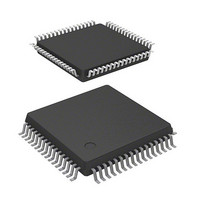
DF71251AD50FPV Renesas Electronics America, DF71251AD50FPV Datasheet - Page 156

DF71251AD50FPV
Manufacturer Part Number
DF71251AD50FPV
Description
MCU RISC FLASH 32K 8K 64LQFP
Manufacturer
Renesas Electronics America
Series
SuperH® SH Tinyr
Datasheet
1.DF71243N50FPV.pdf
(794 pages)
Specifications of DF71251AD50FPV
Core Processor
SH-2
Core Size
32-Bit
Speed
50MHz
Connectivity
SCI
Peripherals
POR, PWM, WDT
Number Of I /o
37
Program Memory Size
32KB (32K x 8)
Program Memory Type
FLASH
Ram Size
8K x 8
Voltage - Supply (vcc/vdd)
4 V ~ 5.5 V
Data Converters
A/D 8x10b
Oscillator Type
External
Operating Temperature
-40°C ~ 85°C
Package / Case
64-LQFP
Lead Free Status / RoHS Status
Lead free / RoHS Compliant
Eeprom Size
-
Available stocks
Company
Part Number
Manufacturer
Quantity
Price
Company:
Part Number:
DF71251AD50FPV
Manufacturer:
Renesas Electronics America
Quantity:
10 000
- Current page: 156 of 794
- Download datasheet (5Mb)
7.3
7.3.1
The flow from setting of break conditions to user break exception processing is described below:
1. The break addresses are set in the break address registers (BARA or BARB). The masked
2. When the break conditions are satisfied, the UBC sends a user break interrupt request to the
3. The appropriate condition match flags (SCMFCA, SCMFDA, SCMFCB, and SCMFDB) can
4. There may be an occasion when a break condition match occurs both in channels A and B
5. When selecting the I bus as the break condition, note the following:
Rev. 5.00 Mar. 06, 2009 Page 136 of 770
REJ09B0243-0500
addresses are set in the break address mask registers (BAMRA or BAMRB). The break data is
set in the break data register (BDRA or BDRB). The masked data is set in the break data mask
register (BDMRA or BDMRB). The bus break conditions are set in the break bus cycle
registers (BBRA or BBRB). Three groups of BBRA or BBRB (L bus cycle/I bus cycle select,
instruction fetch/data access select, and read/write select) are each set. No user break will be
generated if even one of these groups is set with B'00. The respective conditions are set in the
bits of the break control register (BRCR). Make sure to set all registers related to breaks before
setting BBRA or BBRB.
CPU and sets the L bus condition match flag (SCMFCA or SCMFCB) and the I bus condition
match flag (SCMFDA or SCMFDB) for the appropriate channel.
be used to check if the set conditions match or not. The matching of the conditions sets flags,
but they are not reset. Before using them again, 0 must first be written to them and then reset
flags.
around the same time. In this case, the flags for both conditions matches will be set even
though only one user-break interrupt request is issued to the CPU.
⎯ The CPU is connected to the I bus. The UBC monitors bus cycles generated by all bus
⎯ I bus cycles (including read fill cycles) resulting from instruction fetches on the L bus by
⎯ If a break condition is specified for the I bus, even when the condition matches in an I bus
masters that are selected by the CPA2 to CPA0 bits in BBRA or the CPB2 to CPB0 bits in
BBRB, and compares the condition match.
the CPU are defined as instruction fetch cycles on the I bus, while other bus cycles are
defined as data access cycles.
cycle resulting from an instruction executed by the CPU, at which instruction the user-
break is to be accepted cannot be clearly defined.
Operation
Flow of the User Break Operation
Related parts for DF71251AD50FPV
Image
Part Number
Description
Manufacturer
Datasheet
Request
R

Part Number:
Description:
KIT STARTER FOR M16C/29
Manufacturer:
Renesas Electronics America
Datasheet:

Part Number:
Description:
KIT STARTER FOR R8C/2D
Manufacturer:
Renesas Electronics America
Datasheet:

Part Number:
Description:
R0K33062P STARTER KIT
Manufacturer:
Renesas Electronics America
Datasheet:

Part Number:
Description:
KIT STARTER FOR R8C/23 E8A
Manufacturer:
Renesas Electronics America
Datasheet:

Part Number:
Description:
KIT STARTER FOR R8C/25
Manufacturer:
Renesas Electronics America
Datasheet:

Part Number:
Description:
KIT STARTER H8S2456 SHARPE DSPLY
Manufacturer:
Renesas Electronics America
Datasheet:

Part Number:
Description:
KIT STARTER FOR R8C38C
Manufacturer:
Renesas Electronics America
Datasheet:

Part Number:
Description:
KIT STARTER FOR R8C35C
Manufacturer:
Renesas Electronics America
Datasheet:

Part Number:
Description:
KIT STARTER FOR R8CL3AC+LCD APPS
Manufacturer:
Renesas Electronics America
Datasheet:

Part Number:
Description:
KIT STARTER FOR RX610
Manufacturer:
Renesas Electronics America
Datasheet:

Part Number:
Description:
KIT STARTER FOR R32C/118
Manufacturer:
Renesas Electronics America
Datasheet:

Part Number:
Description:
KIT DEV RSK-R8C/26-29
Manufacturer:
Renesas Electronics America
Datasheet:

Part Number:
Description:
KIT STARTER FOR SH7124
Manufacturer:
Renesas Electronics America
Datasheet:

Part Number:
Description:
KIT STARTER FOR H8SX/1622
Manufacturer:
Renesas Electronics America
Datasheet:

Part Number:
Description:
KIT DEV FOR SH7203
Manufacturer:
Renesas Electronics America
Datasheet:


