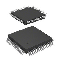
DF71251AD50FPV Renesas Electronics America, DF71251AD50FPV Datasheet - Page 572

DF71251AD50FPV
Manufacturer Part Number
DF71251AD50FPV
Description
MCU RISC FLASH 32K 8K 64LQFP
Manufacturer
Renesas Electronics America
Series
SuperH® SH Tinyr
Datasheet
1.DF71243N50FPV.pdf
(794 pages)
Specifications of DF71251AD50FPV
Core Processor
SH-2
Core Size
32-Bit
Speed
50MHz
Connectivity
SCI
Peripherals
POR, PWM, WDT
Number Of I /o
37
Program Memory Size
32KB (32K x 8)
Program Memory Type
FLASH
Ram Size
8K x 8
Voltage - Supply (vcc/vdd)
4 V ~ 5.5 V
Data Converters
A/D 8x10b
Oscillator Type
External
Operating Temperature
-40°C ~ 85°C
Package / Case
64-LQFP
Lead Free Status / RoHS Status
Lead free / RoHS Compliant
Eeprom Size
-
Available stocks
Company
Part Number
Manufacturer
Quantity
Price
Company:
Part Number:
DF71251AD50FPV
Manufacturer:
Renesas Electronics America
Quantity:
10 000
- Current page: 572 of 794
- Download datasheet (5Mb)
15.2
1. In this LSI, the same function is available as a multiplexed function on multiple pins. This
Table 15.6 Transmit Forms of Input Functions Allocated to Multiple Pins
Note:
2. When the port input is switched from a low level to the IRQ edge for the pins that are
3. Do not set functions other than those specified in tables 15.3 and 15.4. Otherwise, correct
Rev. 5.00 Mar. 06, 2009 Page 552 of 770
REJ09B0243-0500
OR Type
SCK0 to SCK2, RXD0 to RXD2, POE0, POE1,
POE3*, POE8
approach is intended to increase the number of selectable pin functions and to allow the easier
design of boards. If two or more pins are specified for one function, however, there are two
cautions shown below.
⎯ When the pin function is input
⎯ When the pin function is output
multiplexed with input/output and IRQ, the corresponding edge is detected.
operation cannot be guaranteed.
Signals input to several pins are formed as one signal through OR or AND logic and the
signal is transmitted into the LSI. Therefore, a signal that differs from the input signals may
be transmitted to the LSI depending on the input signals in other pins that have the same
functions. Table 15.6 shows the transmit forms of input functions allocated to several pins.
When using one of the functions shown below in multiple pins, use it with care of signal
polarity considering the transmit forms.
OR type:
AND type: Signals input to several pins are formed as one signal through AND logic and
Each selected pin can output the same function.
* This pin is supported only by the SH7125.
Usage Notes
Signals input to several pins are formed as one signal through OR logic and the
signal is transmitted into the LSI.
the signal is transmitted into the LSI.
AND Type
IRQ0* to IRQ3
Related parts for DF71251AD50FPV
Image
Part Number
Description
Manufacturer
Datasheet
Request
R

Part Number:
Description:
KIT STARTER FOR M16C/29
Manufacturer:
Renesas Electronics America
Datasheet:

Part Number:
Description:
KIT STARTER FOR R8C/2D
Manufacturer:
Renesas Electronics America
Datasheet:

Part Number:
Description:
R0K33062P STARTER KIT
Manufacturer:
Renesas Electronics America
Datasheet:

Part Number:
Description:
KIT STARTER FOR R8C/23 E8A
Manufacturer:
Renesas Electronics America
Datasheet:

Part Number:
Description:
KIT STARTER FOR R8C/25
Manufacturer:
Renesas Electronics America
Datasheet:

Part Number:
Description:
KIT STARTER H8S2456 SHARPE DSPLY
Manufacturer:
Renesas Electronics America
Datasheet:

Part Number:
Description:
KIT STARTER FOR R8C38C
Manufacturer:
Renesas Electronics America
Datasheet:

Part Number:
Description:
KIT STARTER FOR R8C35C
Manufacturer:
Renesas Electronics America
Datasheet:

Part Number:
Description:
KIT STARTER FOR R8CL3AC+LCD APPS
Manufacturer:
Renesas Electronics America
Datasheet:

Part Number:
Description:
KIT STARTER FOR RX610
Manufacturer:
Renesas Electronics America
Datasheet:

Part Number:
Description:
KIT STARTER FOR R32C/118
Manufacturer:
Renesas Electronics America
Datasheet:

Part Number:
Description:
KIT DEV RSK-R8C/26-29
Manufacturer:
Renesas Electronics America
Datasheet:

Part Number:
Description:
KIT STARTER FOR SH7124
Manufacturer:
Renesas Electronics America
Datasheet:

Part Number:
Description:
KIT STARTER FOR H8SX/1622
Manufacturer:
Renesas Electronics America
Datasheet:

Part Number:
Description:
KIT DEV FOR SH7203
Manufacturer:
Renesas Electronics America
Datasheet:


