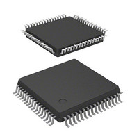
DF71251AD50FPV Renesas Electronics America, DF71251AD50FPV Datasheet - Page 679

DF71251AD50FPV
Manufacturer Part Number
DF71251AD50FPV
Description
MCU RISC FLASH 32K 8K 64LQFP
Manufacturer
Renesas Electronics America
Series
SuperH® SH Tinyr
Datasheet
1.DF71243N50FPV.pdf
(794 pages)
Specifications of DF71251AD50FPV
Core Processor
SH-2
Core Size
32-Bit
Speed
50MHz
Connectivity
SCI
Peripherals
POR, PWM, WDT
Number Of I /o
37
Program Memory Size
32KB (32K x 8)
Program Memory Type
FLASH
Ram Size
8K x 8
Voltage - Supply (vcc/vdd)
4 V ~ 5.5 V
Data Converters
A/D 8x10b
Oscillator Type
External
Operating Temperature
-40°C ~ 85°C
Package / Case
64-LQFP
Lead Free Status / RoHS Status
Lead free / RoHS Compliant
Eeprom Size
-
Available stocks
Company
Part Number
Manufacturer
Quantity
Price
Company:
Part Number:
DF71251AD50FPV
Manufacturer:
Renesas Electronics America
Quantity:
10 000
- Current page: 679 of 794
- Download datasheet (5Mb)
5. The flash memory is not accessible during programming/erasing operations. Therefore, the
6. After programming/erasing, access to flash memory is inhibited until FKEY is cleared.
7. When the program data storage area indicated by the FMPDR parameter in the programming
Tables 17.16 and 17.17 show the areas in which the program data can be stored and executed
according to the operation type and mode.
Table 17.16 Executable MAT
Operation
Programming
Erasing
table, interrupt processing routine, and user branch program should be transferred to on-chip
RAM before programming/erasing of the flash memory starts.
programming/erasing program must be downloaded to on-chip RAM in advance. Areas for
executing each procedure program for initiating programming/erasing, the user program at the
user branch destination for programming/erasing, the interrupt vector table, and the interrupt
processing routine must be located in on-chip RAM.
A reset state (RES = 0) for more than at least 100 μs must be taken when the LSI mode is
changed to reset on completion of a programming/erasing operation.
Transitions to the reset state during programming/erasing are inhibited. When the reset signal
is accidentally input to the LSI, a longer period in the reset state than usual (100 μs) is needed
before the reset signal is released.
processing is within the flash memory area, an error will occur. Therefore, temporarily transfer
the program data to on-chip RAM to change the address set in FMPDR to an address other
than flash memory.
Initiated Mode
User Program Mode
Table 17.17 (1)
Table 17.17 (2)
Rev. 5.00 Mar. 06, 2009 Page 659 of 770
REJ09B0243-0500
Related parts for DF71251AD50FPV
Image
Part Number
Description
Manufacturer
Datasheet
Request
R

Part Number:
Description:
KIT STARTER FOR M16C/29
Manufacturer:
Renesas Electronics America
Datasheet:

Part Number:
Description:
KIT STARTER FOR R8C/2D
Manufacturer:
Renesas Electronics America
Datasheet:

Part Number:
Description:
R0K33062P STARTER KIT
Manufacturer:
Renesas Electronics America
Datasheet:

Part Number:
Description:
KIT STARTER FOR R8C/23 E8A
Manufacturer:
Renesas Electronics America
Datasheet:

Part Number:
Description:
KIT STARTER FOR R8C/25
Manufacturer:
Renesas Electronics America
Datasheet:

Part Number:
Description:
KIT STARTER H8S2456 SHARPE DSPLY
Manufacturer:
Renesas Electronics America
Datasheet:

Part Number:
Description:
KIT STARTER FOR R8C38C
Manufacturer:
Renesas Electronics America
Datasheet:

Part Number:
Description:
KIT STARTER FOR R8C35C
Manufacturer:
Renesas Electronics America
Datasheet:

Part Number:
Description:
KIT STARTER FOR R8CL3AC+LCD APPS
Manufacturer:
Renesas Electronics America
Datasheet:

Part Number:
Description:
KIT STARTER FOR RX610
Manufacturer:
Renesas Electronics America
Datasheet:

Part Number:
Description:
KIT STARTER FOR R32C/118
Manufacturer:
Renesas Electronics America
Datasheet:

Part Number:
Description:
KIT DEV RSK-R8C/26-29
Manufacturer:
Renesas Electronics America
Datasheet:

Part Number:
Description:
KIT STARTER FOR SH7124
Manufacturer:
Renesas Electronics America
Datasheet:

Part Number:
Description:
KIT STARTER FOR H8SX/1622
Manufacturer:
Renesas Electronics America
Datasheet:

Part Number:
Description:
KIT DEV FOR SH7203
Manufacturer:
Renesas Electronics America
Datasheet:


