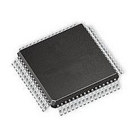
Z16FMC64AG20SG Zilog, Z16FMC64AG20SG Datasheet - Page 230

Z16FMC64AG20SG
Manufacturer Part Number
Z16FMC64AG20SG
Description
Microcontrollers (MCU) 16BIT 64K FL 4K RAM 2UART 12CH 10BIT A/D
Manufacturer
Zilog
Series
Z16FMCr
Datasheet
1.Z16FMC28AG20_EG.pdf
(341 pages)
Specifications of Z16FMC64AG20SG
Processor Series
Z16FMC
Core
ZNEO
Data Bus Width
16 bit
Program Memory Type
Flash
Program Memory Size
64 KB
Data Ram Size
4 KB
Interface Type
I2C, SPI, UART
Maximum Clock Frequency
20 MHz
Number Of Programmable I/os
46
Operating Supply Voltage
2.7 V to 3.6 V
Maximum Operating Temperature
+ 70 C
Mounting Style
SMD/SMT
Package / Case
LQFP-64
Development Tools By Supplier
Z16FMC28200KITG
Minimum Operating Temperature
0 C
Core Processor
ZNEO
Core Size
16-Bit
Speed
20MHz
Connectivity
I²C, IrDA, LIN, SPI, UART/USART
Peripherals
Brown-out Detect/Reset, DMA, POR, PWM, WDT
Number Of I /o
46
Eeprom Size
-
Ram Size
4K x 8
Voltage - Supply (vcc/vdd)
2.7 V ~ 3.6 V
Data Converters
A/D 12x10b
Oscillator Type
Internal
Operating Temperature
0°C ~ 70°C
Lead Free Status / Rohs Status
Details
Available stocks
Company
Part Number
Manufacturer
Quantity
Price
Company:
Part Number:
Z16FMC64AG20SG
Manufacturer:
Zilog
Quantity:
161
- Current page: 230 of 341
- Download datasheet (21Mb)
ADC Control Register Definitions
PS028702-1210
ADC Interrupts
ADC0 Timer0 Capture
ADC Convert on Read
Reference Buffer, RBUF
Internal Voltage Reference Generator
ADC0 Control Register 0
The ADC generates an interrupt request when a conversion has been completed. An inter-
rupt request pending when the ADC is disabled is not automatically cleared.
The Timer0 count is captured for every ADC0 conversion. The information is used to
determine the zero crossing of back EMF in motor control applications. The capture of the
Timer0 count occurs when the programmed sample time is complete for every conversion
and stored in the ADC Timer Capture Register (ADCTCAP).
The ADC is set up to automatically convert the next channel input after reading the results
of the current conversion. The conversions continue up to the channel listed in the
ADC0MAX register and then start over at the initial channel. The initial channel to con-
vert is written to the control register, ADC0CTL, prior to starting the convert on Read pro-
cess. After conversions have started, they continue to loop from the initial channel to Max
channel until the convert on Read bit,
data registers.
The reference buffer, RBUF, supplies the reference voltage for the ADC. When enabled,
the internal voltage reference generator supplies the ADC and the voltage is available on
the VREF pin. When RBUF is disabled, the reference voltage must be supplied externally
through the VREF pin. RBUF is controlled by the REFEN bit in the ADC0 control register.
The internal voltage reference generator provides the voltage to RBUF. The internal refer-
ence voltage is 2 V.
The following sections describe the control registers for the ADC.
The ADC0 Control Register initiates the A/D conversion and provides ADC0 status infor-
mation.
P R E L I M I N A R Y
CVTRD0
, is cleared or the data is not read from the
Z16FMC Series Motor Control MCUs
Product Specification
Analog Functions
208
Related parts for Z16FMC64AG20SG
Image
Part Number
Description
Manufacturer
Datasheet
Request
R

Part Number:
Description:
Microcontrollers (MCU) 16BIT 32K FL 2K RAM 2UART 12CH 10BIT A/D
Manufacturer:
Zilog
Datasheet:

Part Number:
Description:
Microcontrollers (MCU) 16BIT 128K FL 4KRAM 2UART 12CH 10BIT A/D
Manufacturer:
Zilog
Datasheet:

Part Number:
Description:
Microcontrollers (MCU) 16BIT 64K FL 4K RAM 2UART 12CH 10BIT A/D
Manufacturer:
Zilog
Datasheet:

Part Number:
Description:
Microcontrollers (MCU) 16BIT 32K FL 2K RAM 2UART 12CH 10BIT A/D
Manufacturer:
Zilog
Datasheet:

Part Number:
Description:
Microcontrollers (MCU) 16BIT 128K FL 4KRAM 2UART 12CH 10BIT A/D
Manufacturer:
Zilog

Part Number:
Description:
Communication Controllers, ZILOG INTELLIGENT PERIPHERAL CONTROLLER (ZIP)
Manufacturer:
Zilog, Inc.
Datasheet:

Part Number:
Description:
KIT DEV FOR Z8 ENCORE 16K TO 64K
Manufacturer:
Zilog
Datasheet:

Part Number:
Description:
KIT DEV Z8 ENCORE XP 28-PIN
Manufacturer:
Zilog
Datasheet:

Part Number:
Description:
DEV KIT FOR Z8 ENCORE 8K/4K
Manufacturer:
Zilog
Datasheet:

Part Number:
Description:
KIT DEV Z8 ENCORE XP 28-PIN
Manufacturer:
Zilog
Datasheet:

Part Number:
Description:
DEV KIT FOR Z8 ENCORE 4K TO 8K
Manufacturer:
Zilog
Datasheet:

Part Number:
Description:
CMOS Z8 microcontroller. ROM 16 Kbytes, RAM 256 bytes, speed 16 MHz, 32 lines I/O, 3.0V to 5.5V
Manufacturer:
Zilog, Inc.
Datasheet:

Part Number:
Description:
Low-cost microcontroller. 512 bytes ROM, 61 bytes RAM, 8 MHz
Manufacturer:
Zilog, Inc.
Datasheet:

Part Number:
Description:
Z8 4K OTP Microcontroller
Manufacturer:
Zilog, Inc.
Datasheet:


