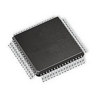
Z16FMC64AG20SG Zilog, Z16FMC64AG20SG Datasheet - Page 136

Z16FMC64AG20SG
Manufacturer Part Number
Z16FMC64AG20SG
Description
Microcontrollers (MCU) 16BIT 64K FL 4K RAM 2UART 12CH 10BIT A/D
Manufacturer
Zilog
Series
Z16FMCr
Datasheet
1.Z16FMC28AG20_EG.pdf
(341 pages)
Specifications of Z16FMC64AG20SG
Processor Series
Z16FMC
Core
ZNEO
Data Bus Width
16 bit
Program Memory Type
Flash
Program Memory Size
64 KB
Data Ram Size
4 KB
Interface Type
I2C, SPI, UART
Maximum Clock Frequency
20 MHz
Number Of Programmable I/os
46
Operating Supply Voltage
2.7 V to 3.6 V
Maximum Operating Temperature
+ 70 C
Mounting Style
SMD/SMT
Package / Case
LQFP-64
Development Tools By Supplier
Z16FMC28200KITG
Minimum Operating Temperature
0 C
Core Processor
ZNEO
Core Size
16-Bit
Speed
20MHz
Connectivity
I²C, IrDA, LIN, SPI, UART/USART
Peripherals
Brown-out Detect/Reset, DMA, POR, PWM, WDT
Number Of I /o
46
Eeprom Size
-
Ram Size
4K x 8
Voltage - Supply (vcc/vdd)
2.7 V ~ 3.6 V
Data Converters
A/D 12x10b
Oscillator Type
Internal
Operating Temperature
0°C ~ 70°C
Lead Free Status / Rohs Status
Details
Available stocks
Company
Part Number
Manufacturer
Quantity
Price
Company:
Part Number:
Z16FMC64AG20SG
Manufacturer:
Zilog
Quantity:
161
- Current page: 136 of 341
- Download datasheet (21Mb)
PS028702-1210
Clear To Send Operation
External Driver Enable
1. Check the LIN-UART Status 0 register to determine whether the source of the inter-
2. If the interrupt was due to data available, read the data from the LIN-UART receive
3. Execute the
The clear to send (CTS) pin, if enabled by the
ister, performs flow control on the outgoing transmit data stream. The CTS input pin is
sampled one system clock before beginning any new character transmission. To delay
transmission of the next data character, an external receiver must deassert CTS at least one
system clock cycle before a new data transmission begins. For multiple character trans-
missions, this operation is typically performed during the Stop bit transmission. If CTS
deasserts in the middle of a character transmission, the current character is sent com-
pletely.
The LIN-UART provides a Driver Enable (DE) signal for off-chip bus transceivers. This
feature reduces the software overhead associated with using a GPIO pin to control the
transceiver when communicating on a multi-transceiver bus such as RS-485.
Driver Enable is a programmable polarity signal which envelopes the entire transmitted
data frame including parity and stop bits as illustrated in Figure 17. The DE signal asserts
when a byte is written to the LIN-UART transmit data register. The DE signal asserts at
least one bit period and no greater than two bit periods before the Start bit is transmitted.
This allows a set-up time to enable the transceiver. The DE signal deasserts one system
clock period after the final
both time for data to clear the transceiver before disabling it, as well as the ability to deter-
mine if another character follows the current character. In the event of back to back char-
acters (new data must be written to the transmit data register before the previous character
is completely transmitted) the DE signal is not deasserted between characters. The
DEPOL bit in the LIN-UART control register 1 sets the polarity of the DE signal.
rupt is error, break, or received data.
data register. If operating in MULTIPROCESSOR (9-bit) mode, further actions are
required depending on the MULTIPROCESSOR mode bits
IRET
instruction to return from the ISR and await more data.
P R E L I M I N A R Y
Stop
bit is transmitted. This one system clock delay allows
CTSE
Z16FMC Series Motor Control MCUs
bit of the LIN-UART Control 0 Reg-
MPMD[1:0]
Product Specification
.
LIN-UART
114
Related parts for Z16FMC64AG20SG
Image
Part Number
Description
Manufacturer
Datasheet
Request
R

Part Number:
Description:
Microcontrollers (MCU) 16BIT 32K FL 2K RAM 2UART 12CH 10BIT A/D
Manufacturer:
Zilog
Datasheet:

Part Number:
Description:
Microcontrollers (MCU) 16BIT 128K FL 4KRAM 2UART 12CH 10BIT A/D
Manufacturer:
Zilog
Datasheet:

Part Number:
Description:
Microcontrollers (MCU) 16BIT 64K FL 4K RAM 2UART 12CH 10BIT A/D
Manufacturer:
Zilog
Datasheet:

Part Number:
Description:
Microcontrollers (MCU) 16BIT 32K FL 2K RAM 2UART 12CH 10BIT A/D
Manufacturer:
Zilog
Datasheet:

Part Number:
Description:
Microcontrollers (MCU) 16BIT 128K FL 4KRAM 2UART 12CH 10BIT A/D
Manufacturer:
Zilog

Part Number:
Description:
Communication Controllers, ZILOG INTELLIGENT PERIPHERAL CONTROLLER (ZIP)
Manufacturer:
Zilog, Inc.
Datasheet:

Part Number:
Description:
KIT DEV FOR Z8 ENCORE 16K TO 64K
Manufacturer:
Zilog
Datasheet:

Part Number:
Description:
KIT DEV Z8 ENCORE XP 28-PIN
Manufacturer:
Zilog
Datasheet:

Part Number:
Description:
DEV KIT FOR Z8 ENCORE 8K/4K
Manufacturer:
Zilog
Datasheet:

Part Number:
Description:
KIT DEV Z8 ENCORE XP 28-PIN
Manufacturer:
Zilog
Datasheet:

Part Number:
Description:
DEV KIT FOR Z8 ENCORE 4K TO 8K
Manufacturer:
Zilog
Datasheet:

Part Number:
Description:
CMOS Z8 microcontroller. ROM 16 Kbytes, RAM 256 bytes, speed 16 MHz, 32 lines I/O, 3.0V to 5.5V
Manufacturer:
Zilog, Inc.
Datasheet:

Part Number:
Description:
Low-cost microcontroller. 512 bytes ROM, 61 bytes RAM, 8 MHz
Manufacturer:
Zilog, Inc.
Datasheet:

Part Number:
Description:
Z8 4K OTP Microcontroller
Manufacturer:
Zilog, Inc.
Datasheet:


