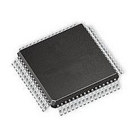
Z16FMC64AG20SG Zilog, Z16FMC64AG20SG Datasheet - Page 176

Z16FMC64AG20SG
Manufacturer Part Number
Z16FMC64AG20SG
Description
Microcontrollers (MCU) 16BIT 64K FL 4K RAM 2UART 12CH 10BIT A/D
Manufacturer
Zilog
Series
Z16FMCr
Datasheet
1.Z16FMC28AG20_EG.pdf
(341 pages)
Specifications of Z16FMC64AG20SG
Processor Series
Z16FMC
Core
ZNEO
Data Bus Width
16 bit
Program Memory Type
Flash
Program Memory Size
64 KB
Data Ram Size
4 KB
Interface Type
I2C, SPI, UART
Maximum Clock Frequency
20 MHz
Number Of Programmable I/os
46
Operating Supply Voltage
2.7 V to 3.6 V
Maximum Operating Temperature
+ 70 C
Mounting Style
SMD/SMT
Package / Case
LQFP-64
Development Tools By Supplier
Z16FMC28200KITG
Minimum Operating Temperature
0 C
Core Processor
ZNEO
Core Size
16-Bit
Speed
20MHz
Connectivity
I²C, IrDA, LIN, SPI, UART/USART
Peripherals
Brown-out Detect/Reset, DMA, POR, PWM, WDT
Number Of I /o
46
Eeprom Size
-
Ram Size
4K x 8
Voltage - Supply (vcc/vdd)
2.7 V ~ 3.6 V
Data Converters
A/D 12x10b
Oscillator Type
Internal
Operating Temperature
0°C ~ 70°C
Lead Free Status / Rohs Status
Details
Available stocks
Company
Part Number
Manufacturer
Quantity
Price
Company:
Part Number:
Z16FMC64AG20SG
Manufacturer:
Zilog
Quantity:
161
- Current page: 176 of 341
- Download datasheet (21Mb)
PS028702-1210
SCK (SSMD = 00,
Rx Data Register
Tx Data Register
Shift Register
MOSI, MISO
ESPI Interrupt
CLKPOL = 0,
PHASE = 0,
SSPO = 0)
RDRF
TDRE
I
Inter-Integrated Circuit Sound mode (I
mode register to 010. The
This mode is illustrated in Figure 29 with SS alternating between consecutive frames. A
frame consists of a fixed number of data bytes as defined in the DMA buffer descriptor or
by software. I
The SSV indicates whether the corresponding bytes are left or right channel data. The
SSV value must be updated when servicing the TDRE interrupt/request for the first byte in
a left or write channel frame. Servicing this request is accomplished by performing a word
write when writing the first byte of the audio word, which updates both the ESPI data and
transmit data command words or by doing a byte write to update SSV followed by a byte
write to the data register. The SS signal leads the data by one SCK period.
If a DMA channel is controlling data transfer, each sequence of left (or right) channel byte
is considered a frame with a buffer descriptor. The SSV bit is defined in the buffer descrip-
tor command field and is automatically written to the transmit data command register just
prior to or in synchronous with the first data byte of the frame being written. Note that the
2
S Mode
Tx/Rx n–1
Tx n
Bit0
2
S mode is typically used to transfer left or right channel audio data.
Rx n–1
Bit7
Figure 28. SPI mode (SSMD = 000)
Bit6
Phase
P R E L I M I N A R Y
and
CLKPOL
Tx/Rx n
2
Tx n+1
S) is selected by setting the SSMD field of the
Empty
bits of the control register must be set to 0.
Z16FMC Series Motor Control MCUs
Bit1
Enhanced Serial Peripheral Interface
Bit0
Product Specification
Bit7
Rx n
Tx/Rx n+1
Bit 6
empty
Tx n+2
154
Related parts for Z16FMC64AG20SG
Image
Part Number
Description
Manufacturer
Datasheet
Request
R

Part Number:
Description:
Microcontrollers (MCU) 16BIT 32K FL 2K RAM 2UART 12CH 10BIT A/D
Manufacturer:
Zilog
Datasheet:

Part Number:
Description:
Microcontrollers (MCU) 16BIT 128K FL 4KRAM 2UART 12CH 10BIT A/D
Manufacturer:
Zilog
Datasheet:

Part Number:
Description:
Microcontrollers (MCU) 16BIT 64K FL 4K RAM 2UART 12CH 10BIT A/D
Manufacturer:
Zilog
Datasheet:

Part Number:
Description:
Microcontrollers (MCU) 16BIT 32K FL 2K RAM 2UART 12CH 10BIT A/D
Manufacturer:
Zilog
Datasheet:

Part Number:
Description:
Microcontrollers (MCU) 16BIT 128K FL 4KRAM 2UART 12CH 10BIT A/D
Manufacturer:
Zilog

Part Number:
Description:
Communication Controllers, ZILOG INTELLIGENT PERIPHERAL CONTROLLER (ZIP)
Manufacturer:
Zilog, Inc.
Datasheet:

Part Number:
Description:
KIT DEV FOR Z8 ENCORE 16K TO 64K
Manufacturer:
Zilog
Datasheet:

Part Number:
Description:
KIT DEV Z8 ENCORE XP 28-PIN
Manufacturer:
Zilog
Datasheet:

Part Number:
Description:
DEV KIT FOR Z8 ENCORE 8K/4K
Manufacturer:
Zilog
Datasheet:

Part Number:
Description:
KIT DEV Z8 ENCORE XP 28-PIN
Manufacturer:
Zilog
Datasheet:

Part Number:
Description:
DEV KIT FOR Z8 ENCORE 4K TO 8K
Manufacturer:
Zilog
Datasheet:

Part Number:
Description:
CMOS Z8 microcontroller. ROM 16 Kbytes, RAM 256 bytes, speed 16 MHz, 32 lines I/O, 3.0V to 5.5V
Manufacturer:
Zilog, Inc.
Datasheet:

Part Number:
Description:
Low-cost microcontroller. 512 bytes ROM, 61 bytes RAM, 8 MHz
Manufacturer:
Zilog, Inc.
Datasheet:

Part Number:
Description:
Z8 4K OTP Microcontroller
Manufacturer:
Zilog, Inc.
Datasheet:


