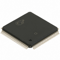
CY7C67300-100AXA Cypress Semiconductor Corp, CY7C67300-100AXA Datasheet - Page 53

CY7C67300-100AXA
Manufacturer Part Number
CY7C67300-100AXA
Description
IC,Peripheral (Multifunction) Controller,QFP,100PIN
Manufacturer
Cypress Semiconductor Corp
Series
EZ-Host™r
Datasheet
1.CY7C67300-100AXA.pdf
(98 pages)
Specifications of CY7C67300-100AXA
Applications
USB Host/Peripheral Controller
Core Processor
CY16
Program Memory Type
ROM (8 kB)
Controller Series
CY7C673xx
Ram Size
16K x 8
Interface
SPI Serial, USB, HPI
Number Of I /o
32
Voltage - Supply
3 V ~ 3.6 V
Operating Temperature
-40°C ~ 85°C
Mounting Type
Surface Mount
Package / Case
100-LQFP
Lead Free Status / RoHS Status
Lead free / RoHS Compliant
For Use With
CY4640 - KIT MASS STORAGE REF DESIGNCY3663 - KIT DEV EZ-OTG/EZ-HOST
Lead Free Status / RoHS Status
Lead free / RoHS Compliant
Available stocks
Company
Part Number
Manufacturer
Quantity
Price
Company:
Part Number:
CY7C67300-100AXA
Manufacturer:
Cypress Semiconductor Corp
Quantity:
10 000
Company:
Part Number:
CY7C67300-100AXAT
Manufacturer:
Cypress Semiconductor Corp
Quantity:
10 000
Document #: 38-08015 Rev. *G
Table 40.Mode Select Definition
Reserved
All reserved bits should be written as ‘0’.
IDE Start Address Register [0xC04A] [R/W]
Register Description
The IDE Start Address Register holds the start address for an IDE block transfer. This register is byte addressed and IDE block
transfers are 16-bit words, therefore the LSB of the start address is ignored. Block transfers begin at IDE Start Address and end
with the final word at IDE Stop Address. When IDE Start Address equals IDE Stop Address, the block transfer moves one word
of data.
The hardware keeps an internal memory address counter. The two MSBs of the addresses are not modified by the address
counter. Therefore, the IDE Start Address and IDE Stop Address must reside within the same 16-Kbyte block.
Address (Bits [15:0])
The Address field sets the start address for an IDE block transfer.
IDE Stop Address Register [0xC04C] [R/W]
Bit #
Field
Read/Write
Default
Bit #
Field
Read/Write
Default
Bit #
Field
Read/Write
Default
Bit #
Field
Read/Write
Default
Mode Select [2:0]
000
001
010
100
101
011
110
111
R/W
R/W
R/W
R/W
15
15
0
7
0
0
7
0
R/W
R/W
R/W
R/W
14
14
0
6
0
0
6
0
Figure 55. IDE Start Address Register
Figure 56. IDE Stop Address Register
R/W
R/W
R/W
R/W
13
13
0
5
0
0
5
0
Disable IDE port operations
IDE PIO Mode 0
IDE PIO Mode 1
IDE PIO Mode 2
IDE PIO Mode 3
IDE PIO Mode 4
R/W
R/W
R/W
R/W
12
12
0
4
0
0
4
0
Reserved
Reserved
Mode
Address...
...Address
Address...
...Address
R/W
R/W
R/W
R/W
11
11
0
3
0
0
3
0
R/W
R/W
R/W
R/W
10
10
0
2
0
0
2
0
R/W
R/W
R/W
R/W
9
0
1
0
9
0
1
0
CY7C67300
Page 53 of 98
R/W
R/W
R/W
R/W
8
0
0
0
8
0
0
0
[+] Feedback


