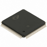
CY7C67300-100AXA Cypress Semiconductor Corp, CY7C67300-100AXA Datasheet - Page 5

CY7C67300-100AXA
Manufacturer Part Number
CY7C67300-100AXA
Description
IC,Peripheral (Multifunction) Controller,QFP,100PIN
Manufacturer
Cypress Semiconductor Corp
Series
EZ-Host™r
Datasheet
1.CY7C67300-100AXA.pdf
(98 pages)
Specifications of CY7C67300-100AXA
Applications
USB Host/Peripheral Controller
Core Processor
CY16
Program Memory Type
ROM (8 kB)
Controller Series
CY7C673xx
Ram Size
16K x 8
Interface
SPI Serial, USB, HPI
Number Of I /o
32
Voltage - Supply
3 V ~ 3.6 V
Operating Temperature
-40°C ~ 85°C
Mounting Type
Surface Mount
Package / Case
100-LQFP
Lead Free Status / RoHS Status
Lead free / RoHS Compliant
For Use With
CY4640 - KIT MASS STORAGE REF DESIGNCY3663 - KIT DEV EZ-OTG/EZ-HOST
Lead Free Status / RoHS Status
Lead free / RoHS Compliant
Available stocks
Company
Part Number
Manufacturer
Quantity
Price
Company:
Part Number:
CY7C67300-100AXA
Manufacturer:
Cypress Semiconductor Corp
Quantity:
10 000
Company:
Part Number:
CY7C67300-100AXAT
Manufacturer:
Cypress Semiconductor Corp
Quantity:
10 000
Document #: 38-08015 Rev. *G
External Memory Interface
EZ-Host provides a robust interface to a wide variety of
external memory arrays. All available external memory array
locations can contain either code or data. The CY16 RISC
processor directly addresses a flat memory space from
0x0000 to 0xFFFF.
External Memory Interface Features
External Memory Access Strobes
Access to external memory is sampled asynchronously on the
rising edge of strobes with a minimum of one wait state cycle.
Up to seven wait state cycles may be inserted for external
Merge Mode
Merge modes enabled through the External Memory Control
Register [0xC03A] allow combining of external memory
regions in accordance with the following:
Program Memory Hole Description
Code residing in the 0xC000-0xC0FF address space is not
accessible by the CPU.
DMA to External Memory Prohibited
EZ-Host supports an internal DMA engine to rapidly move data
between different functional blocks within the chip. This DMA
engine is used for SIE1, SIE2, HPI, SPI, HSS, and IDE but it
can only transfer data between the specified block and internal
RAM or ROM. Setting up the DMA engine to transfer to or from
an external memory space might result in internal RAM data
• Supports 8-bit or 16-bit SRAM or ROM
• SRAM or ROM can be used for code or data space
• Direct addressing of SRAM or ROM
• Two external memory mapped page registers
• nXMEMSEL is active from 0x8000 to 0xBFFF
• nXRAMSEL is active from 0x4000 to 0x7FFF when RAM
• nXROMSEL is active from 0xC100 to 0xDFFF when ROM
Merge is disabled; nXRAMSEL is active from 0x4000 to
0xBFFF when RAM Merge is enabled
Merge is disabled; nXROMSEL is active from 0x8000 to
0xDFFF (excluding the 0xC000 to 0xC0FF area) when ROM
Merge is enabled
Where:
PAGEx Register[5:0] + PC[12:0]
PC = Program Counter
x = 1 or 2
A = CPU Address Bus
Figure 1. Page n Registers External Address Pins Logic
0000 + PC[14:0]
nXMEMSEL Pin
Note:
1
0
PAGE 1 Register Active Range = 8000h to 9FFFh
PAGE 2 Register Active Range = A000h to BFFFh
nXMEMSEL Pin Active Range = 8000h to BFFFh
memory access. Each additional wait state cycle stretches the
external memory access time by 21 ns (you must be running
in internal memory when changing wait states). An external
memory device with 12-ns access time is necessary to support
48-MHz code execution.
Page Registers
EZ-Host allows extended data or program code to be stored in
external SRAM, or ROM. The total size of extended memory
can be up to 512K bytes. The CY16 processor can access
extended memory via two address regions of 0x8000-0x9FFF
and 0xA000-0xBFFF. The page register 0xC018 can be used
to control the address region 0x8000-0x9FFF and the page
register
0xA000-0xBFFF.
Figure 1
the upper CPU address pins are driven by the contents of the
Page x Registers.
corruption
HSS/HPI/SIE1/SIE2/IDE) does not explicitly check the
address range. For example, setting up a DMA transfer to
external address 0x8000 might result in a DMA transfer into
address 0x0000.
External Memory Related Resource Considerations:
A[18:0]
• By default A[18:15] are not available for general addressing
• 47k ohm external pull up on A15-pin for 12-MHz crystal
• During the 3-ms BIOS boot procedure the CPU external
• ROM boot load value 0xC3B6 located at 0xC100.
• HPI, HSS, SPI, SIE1, SIE2, and IDE can't DMA to external
• Page 1 banking is always enabled and is in effect from
• Page 2 banking is always enabled and is in effect from
• CPU memory bus strobes may wiggle when chip selects
and are driven high on power up. The Upper Address
Enable Register must be written appropriately to enable
A[18:15] for general addressing purposes.
operation.
memory bus is active.
memory arrays.
0x8000 to 0x9FFF.
0xA000 to 0xBFFF.
are inactive.
illustrates that when the nXMEMSEL pin is asserted
0xC01A
because
controls
the
hardware
the
address
CY7C67300
(for
Page 5 of 98
region
example,
of
[+] Feedback


