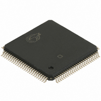
CY7C67300-100AXA Cypress Semiconductor Corp, CY7C67300-100AXA Datasheet - Page 50

CY7C67300-100AXA
Manufacturer Part Number
CY7C67300-100AXA
Description
IC,Peripheral (Multifunction) Controller,QFP,100PIN
Manufacturer
Cypress Semiconductor Corp
Series
EZ-Host™r
Datasheet
1.CY7C67300-100AXA.pdf
(98 pages)
Specifications of CY7C67300-100AXA
Applications
USB Host/Peripheral Controller
Core Processor
CY16
Program Memory Type
ROM (8 kB)
Controller Series
CY7C673xx
Ram Size
16K x 8
Interface
SPI Serial, USB, HPI
Number Of I /o
32
Voltage - Supply
3 V ~ 3.6 V
Operating Temperature
-40°C ~ 85°C
Mounting Type
Surface Mount
Package / Case
100-LQFP
Lead Free Status / RoHS Status
Lead free / RoHS Compliant
For Use With
CY4640 - KIT MASS STORAGE REF DESIGNCY3663 - KIT DEV EZ-OTG/EZ-HOST
Lead Free Status / RoHS Status
Lead free / RoHS Compliant
Available stocks
Company
Part Number
Manufacturer
Quantity
Price
Company:
Part Number:
CY7C67300-100AXA
Manufacturer:
Cypress Semiconductor Corp
Quantity:
10 000
Company:
Part Number:
CY7C67300-100AXAT
Manufacturer:
Cypress Semiconductor Corp
Quantity:
10 000
Document #: 38-08015 Rev. *G
SAS Enable (Bit 11)
The SAS Enable bit, when in SPI mode, reroutes the SPI port
SPI_nSSI pin to GPIO[15] rather then GPIO[9] or XD[9] (per
SG/SX).
1: Reroute SPI_nss to GPIO[30]
0: Leave SPI_nss on GPIO[9]
Mode Select (Bits [10:8])
The Mode Select field selects how GPIO[15:0] and
GPIO[24:19] are used as defined in
Table 38.Mode Select Definition
HSS Enable (Bit 7)
The HSS Enable bit routes HSS to GPIO[26, 18:16]. If the HSS
XD Enable bit is set, it will override this bit and HSS will be
routed to XD[15:12].
1: HSS is routed to GPIO
0: HSS is not routed to GPIOs. GPIO[26, 18:16] are free for
other purposes
HSS XD Enable (Bit 6)
The HSS XD Enable bit routes HSS to XD[15:12] (external
memory data bus). This bit overrides the HSS Enable bit.
1: HSS is routed to XD[15:12]
0: HSS is not routed to XD[15:12]
SPI Enable (Bit 5)
The SPI Enable bit routes SPI to GPIO[11:8]. If the SAS
Enable bit is set, it will override the SPI Enable and route
Mode Select
[10:8]
110
101
100
011
010
001
000
111
Reserved
SCAN — (HW) Scan diagnostic. For produc-
tion test only. Not for normal operation
HPI — Host Port Interface
IDE — Integrated Drive Electronics or
Reserved
Reserved
Reserved
GPIO — General Purpose Input Output
GPIO Configuration
Table
38.
SPI_nSSI to GPIO15. If the SPI XD Enable bit is set, it will
override both bits and the SPI will be routed to XD[11:8]
(external memory data bus).
1: SPI is routed to GPIO[11:8]
0: SPI is not routed to GPIO[11:8]. GPIO[11:8] are free for
other purposes
SPI XD Enable (Bit 4)
The SPI XD Enable bit routes SPI to XD[11:8] (external
memory data bus). This bit overrides the SPI Enable bit.
1: SPI is routed to XD[11:8]
0: SPI is not routed to XD[11:8]
Interrupt 1 Polarity Select (Bit 3)
The Interrupt 1 Polarity Select bit selects the polarity for IRQ1.
1: Sets IRQ1 to rising edge
0: Sets IRQ1 to falling edge
Interrupt 1 Enable (Bit 2)
The Interrupt 1 Enable bit enables or disables IRQ1. The GPIO
bit on the interrupt Enable Register must also be set in order
for this for this interrupt to be enabled.
1: Enable IRQ1
0: Disable IRQ1
Interrupt 0 Polarity Select (Bit 1)
The Interrupt 0 Polarity Select bit selects the polarity for IRQ0.
1: Sets IRQ0 to rising edge
0: Sets IRQ0 to falling edge
Interrupt 0 Enable (Bit 0)
The Interrupt 0 Enable bit enables or disables IRQ0. The GPIO
bit on the interrupt Enable Register must also be set in order
for this for this interrupt to be enabled.
1: Enable IRQ0
0: Disable IRQ0
Reserved
All reserved bits should be written as ‘0’.
CY7C67300
Page 50 of 98
[+] Feedback


