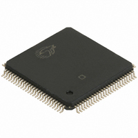
CY7C67300-100AXA Cypress Semiconductor Corp, CY7C67300-100AXA Datasheet - Page 20

CY7C67300-100AXA
Manufacturer Part Number
CY7C67300-100AXA
Description
IC,Peripheral (Multifunction) Controller,QFP,100PIN
Manufacturer
Cypress Semiconductor Corp
Series
EZ-Host™r
Datasheet
1.CY7C67300-100AXA.pdf
(98 pages)
Specifications of CY7C67300-100AXA
Applications
USB Host/Peripheral Controller
Core Processor
CY16
Program Memory Type
ROM (8 kB)
Controller Series
CY7C673xx
Ram Size
16K x 8
Interface
SPI Serial, USB, HPI
Number Of I /o
32
Voltage - Supply
3 V ~ 3.6 V
Operating Temperature
-40°C ~ 85°C
Mounting Type
Surface Mount
Package / Case
100-LQFP
Lead Free Status / RoHS Status
Lead free / RoHS Compliant
For Use With
CY4640 - KIT MASS STORAGE REF DESIGNCY3663 - KIT DEV EZ-OTG/EZ-HOST
Lead Free Status / RoHS Status
Lead free / RoHS Compliant
Available stocks
Company
Part Number
Manufacturer
Quantity
Price
Company:
Part Number:
CY7C67300-100AXA
Manufacturer:
Cypress Semiconductor Corp
Quantity:
10 000
Company:
Part Number:
CY7C67300-100AXAT
Manufacturer:
Cypress Semiconductor Corp
Quantity:
10 000
Document #: 38-08015 Rev. *G
Boost 3V OK (Bit 2)
The Boost 3V OK bit is a read only bit that returns the status
of the OTG Boost circuit.
1: Boost circuit not ok and internal voltage rails are below 3.0V
0: Boost circuit ok and internal voltage rails are at or above
3.0V
Sleep Enable (Bit 1)
Setting this bit to ‘1’ immediately initiates SLEEP mode. While
in SLEEP mode, the entire chip is paused, achieving the
lowest standby power state. All operations are paused, the
internal clock is stopped, the booster circuit and OTG VBUS
charge pump are all powered down, and the USB transceivers
are powered down. All counters and timers are paused but will
retain their values; enabled PWM outputs freeze in their
current states. SLEEP mode exits by any activity selected in
this register. When SLEEP mode ends, instruction execution
resumes within 0.5 ms.
1: Enable Sleep mode
0: No function
Interrupt Enable Register [0xC00E] [R/W]
Register Description
The Interrupt Enable Register allows control of the hardware
interrupt vectors.
OTG Interrupt Enable (Bit 12)
The OTG Interrupt Enable bit enables or disables the OTG
ID/OTG4.4V Valid hardware interrupt.
1: Enable OTG interrupt
0: Disable OTG interrupt
SPI Interrupt Enable (Bit 11)
The SPI Interrupt Enable bit enables or disables the following
three SPI hardware interrupts: SPI TX, SPI RX, and SPI DMA
Block Done.
1: Enable SPI interrupt
0: Disable SPI interrupt
Bit #
Field
Read/Write
Default
Bit #
Field
Read/Write
Default
Interrupt
Enable
HSS
R/W
15
0
7
0
-
In Mailbox
Reserved
Interrupt
Enable
R/W
14
0
6
0
-
Out Mailbox
Figure 16. Interrupt Enable Register
Interrupt
Enable
R/W
13
0
5
0
-
Reserved
Interrupt
Enable
OTG
R/W
12
0
4
1
-
Halt Enable (Bit 0)
Setting this bit to ‘1’ immediately initiates HALT mode. While
in HALT mode, only the CPU is stopped. The internal clock still
runs and all peripherals still operate, including the USB
engines. The power saving using HALT in most cases will be
minimal, but in applications that are very CPU intensive the
incremental savings may provide some benefit.
The HALT state is exited when any enabled interrupt is
triggered. Upon exiting the HALT state, one or two instructions
immediately following the HALT instruction may be executed
before the waking interrupt is serviced (you may want to follow
the HALT instruction with two NOPs).
1: Enable Halt mode
0: No function
Reserved
All reserved bits should be written as ‘0’.
Host/Device 2 Interrupt Enable (Bit 9)
The Host/Device 2 Interrupt Enable bit enables or disables all
of the following Host/Device 2 hardware interrupts: Host 2
USB
Wakeup/Insert/Remove, Device 2 Reset, Device 2 SOF/EOP
or WakeUp from USB, Device 2 Endpoint n.
1: Enable Host 2 and Device 2 interrupt
0: Disable Host 2 and Device 2 interrupt
Host/Device 1 Interrupt Enable (Bit 8)
The Host/Device 1 Interrupt Enable bit enables or disables all
of the following Host/Device 1 hardware interrupts: Host 1
USB
Wakeup/Insert/Remove, Device 1 Reset, Device 1 SOF/EOP
or WakeUp from USB, Device 1Endpoint n.
1: Enable Host 1 and Device 1 interrupt
0: Disable Host 1 and Device 1 interrupt
Done,
Done,
Interrupt
Interrupt
Enable
Enable
UART
R/W
R/W
SPI
11
0
3
0
Host
Host
Reserved
Interrupt
Enable
GPIO
R/W
10
0
2
0
2
1
-
USB
USB
Host/Device 2
Interrupt
Interrupt
Timer 1
Enable
Enable
R/W
R/W
SOF/EOP,
SOF/EOP,
9
0
1
0
CY7C67300
Page 20 of 98
Host/Device 1
Interrupt
Interrupt
Timer 0
Enable
Enable
Host
Host
R/W
R/W
8
0
0
0
2
1
[+] Feedback


