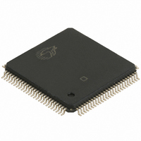
CY7C67300-100AXA Cypress Semiconductor Corp, CY7C67300-100AXA Datasheet - Page 49

CY7C67300-100AXA
Manufacturer Part Number
CY7C67300-100AXA
Description
IC,Peripheral (Multifunction) Controller,QFP,100PIN
Manufacturer
Cypress Semiconductor Corp
Series
EZ-Host™r
Datasheet
1.CY7C67300-100AXA.pdf
(98 pages)
Specifications of CY7C67300-100AXA
Applications
USB Host/Peripheral Controller
Core Processor
CY16
Program Memory Type
ROM (8 kB)
Controller Series
CY7C673xx
Ram Size
16K x 8
Interface
SPI Serial, USB, HPI
Number Of I /o
32
Voltage - Supply
3 V ~ 3.6 V
Operating Temperature
-40°C ~ 85°C
Mounting Type
Surface Mount
Package / Case
100-LQFP
Lead Free Status / RoHS Status
Lead free / RoHS Compliant
For Use With
CY4640 - KIT MASS STORAGE REF DESIGNCY3663 - KIT DEV EZ-OTG/EZ-HOST
Lead Free Status / RoHS Status
Lead free / RoHS Compliant
Available stocks
Company
Part Number
Manufacturer
Quantity
Price
Company:
Part Number:
CY7C67300-100AXA
Manufacturer:
Cypress Semiconductor Corp
Quantity:
10 000
Company:
Part Number:
CY7C67300-100AXAT
Manufacturer:
Cypress Semiconductor Corp
Quantity:
10 000
Document #: 38-08015 Rev. *G
D– Pull-down Enable (Bit 6)
The D– Pull-down Enable bit enables or disables a pull-down
resistor on the OTG D– data line.
1: OTG D– dataline pull-down resistor enabled
0: OTG D– dataline pull-down resistor disabled
OTG Data Status (Bit 2)
The OTG Data Status bit is a read-only bit and indicates the
TTL logic state of the OTG VBus pin.
1: OTG VBus is greater then 2.4V
0: OTG VBus is less then 0.8V
ID Status (Bit 1)
The ID Status bit is a read-only bit that indicates the state of
the OTG ID pin on Port A.
GPIO Registers
There are seven registers dedicated for GPIO operations. These seven registers are covered in this section and summarized in
Table
Table 37.GPIO Registers
GPIO Control Register [0xC006] [R/W]
Register Description
The GPIO Control Register configures the GPIO pins for
various interface options. It also controls the polarity of the
GPIO interrupt on IRQ1 (GPIO25) and IRQ0 (GPIO24).
Write Protect Enable (Bit 15)
The Write Protect Enable bit enables or disables the GPIO
write protect. When Write Protect is enabled, the GPIO Mode
Select [15:8] field is read-only until a chip reset.
GPIO Control Register
GPIO0 Output Data Register
GPIO0 Input Data Register
GPIO0 Direction Register
GPIO1 Output Data Register
GPIO1 Input Data Register
GPIO1 Direction Register
Bit #
Field
Read/Write
Default
Bit #
Field
Read/Write
Default
37.
Write Protect
Enable
Enable
HSS
R/W
R/W
15
0
7
0
Register Name
HSS XD
Enable
R/W
R/W
UD
14
0
6
0
Figure 50. GPIO Control Register
Enable
R/W
SPI
13
0
5
0
-
Reserved
SPI XD
Enable
R/W
12
0
4
0
-
1: OTG ID Pin is not connected directly to ground (>10 kΩ)
0: OTG ID Pin is connected directly ground (< 10Ω)
VBUS Valid Flag (Bit 0)
The VBUS Valid Flag bit indicates whether OTG VBus is
greater then 4.4V. After turning on VBUS, firmware should wait
at least 10 µs before this reading this bit.
1: OTG VBus is greater then 4.4V
0: OTG VBus is less then 4.4V
Reserved
All reserved bits should bit written as ‘0’.
1: Enable Write Protect
0: Disable Write Protect
UD (Bit 14)
The UD bit routes the Host/Device 1A Port’s transmitter enable
status to GPIO[30]. This is for use with an external ESD
protection circuit when needed.
1: Route the signal to GPIO[30]
0: Do not route the signal to GPIO[30]
Polarity Select
Interrupt 1
0xC006
0xC01E
0xC020
0xC022
0xC024
0xC026
0xC028
Enable
SAS
R/W
R/W
11
0
3
0
Address
Interrupt 1
Enable
R/W
R/W
10
0
2
0
Polarity Select
Interrupt 0
Select
R/W
R/W
R
R/W
R/W
R
R/W
Mode
R/W
R/W
9
0
1
0
CY7C67300
Page 49 of 98
R/W
Interrupt 0
Enable
R/W
R/W
8
0
0
0
[+] Feedback


