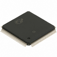
CY7C67300-100AXA Cypress Semiconductor Corp, CY7C67300-100AXA Datasheet - Page 27

CY7C67300-100AXA
Manufacturer Part Number
CY7C67300-100AXA
Description
IC,Peripheral (Multifunction) Controller,QFP,100PIN
Manufacturer
Cypress Semiconductor Corp
Series
EZ-Host™r
Datasheet
1.CY7C67300-100AXA.pdf
(98 pages)
Specifications of CY7C67300-100AXA
Applications
USB Host/Peripheral Controller
Core Processor
CY16
Program Memory Type
ROM (8 kB)
Controller Series
CY7C673xx
Ram Size
16K x 8
Interface
SPI Serial, USB, HPI
Number Of I /o
32
Voltage - Supply
3 V ~ 3.6 V
Operating Temperature
-40°C ~ 85°C
Mounting Type
Surface Mount
Package / Case
100-LQFP
Lead Free Status / RoHS Status
Lead free / RoHS Compliant
For Use With
CY4640 - KIT MASS STORAGE REF DESIGNCY3663 - KIT DEV EZ-OTG/EZ-HOST
Lead Free Status / RoHS Status
Lead free / RoHS Compliant
Available stocks
Company
Part Number
Manufacturer
Quantity
Price
Company:
Part Number:
CY7C67300-100AXA
Manufacturer:
Cypress Semiconductor Corp
Quantity:
10 000
Company:
Part Number:
CY7C67300-100AXAT
Manufacturer:
Cypress Semiconductor Corp
Quantity:
10 000
Document #: 38-08015 Rev. *G
Timer n Register [R/W]
Register Description
The Timer n Register sets the Timer n count. Both Timer 0 and
Timer 1 decrement by one every 1-µs clock tick. Each can
provide an interrupt to the CPU when the timer reaches zero.
General USB Registers
There is one set of registers dedicated to general USB control. This set consists of two identical registers: one for Host/Device
Port 1 and one for Host/Device Port 2. This register set has functions for both USB host and USB peripheral options and is covered
in this section and summarized in
device-only registers are covered in
Table 29.General USB Registers
USB n Control Register [R/W]
Register Description
The USB n Control Register is used in both host and device
mode. It monitors and controls the SIE and the data lines of
the USB ports. This register can be accessed by the HPI
interface.
Bit #
Field
Read/Write
Default
Bit #
Field
Read/Write
Default
USB n Control Register
Bit #
Field
Read/Write
Default
Bit #
Field
Read/Write
Default
• Timer 0 Register 0xC010.
• Timer 1 Register 0xC012.
• USB 1 Control Register 0xC08A.
• USB 2 Control Register 0xC0AA.
Register Name
Resistors
Enable
Port B
Status
Port A
R/W
R/W
R/W
D+
15
15
R
X
1
7
1
7
0
Port B
Status
R/W
R/W
R/W
14
D–
14
R
X
1
6
1
6
0
Table
External Memory Registers on page
Force D±
Port B
State
29. USB Host only registers are covered in
0xC08A/0xC0AA
Figure 25. USB n Control Register
Port A
Status
R/W
R/W
R/W
13
D+
13
R
X
Figure 24. Timer n Register
1
5
1
5
0
Address (SIE1/SIE2)
Port A
Status
R/W
R/W
R/W
12
D–
12
4
1
R
1
X
4
0
Count (Bits [15:0])
The Count field sets the Timer count.
Port B D+ Status (Bit 15)
The Port B D+ Status bit is a read-only bit that indicates the
value of DATA+ on Port B.
1: D+ is HIGH
0: D+ is LOW
Force D±
Count...
...Count
Port A
State
23.
R/W
R/W
LOB
R/W
R/W
11
11
3
1
1
0
3
0
Suspend
UART Interface on page
Enable
R/W
R/W
LOA
R/W
R/W
10
10
2
1
1
0
2
0
SOF/EOP
Enable
Port B
Select
Mode
R/W
R/W
R/W
R/W
1
1
9
1
9
0
1
0
CY7C67300
R/W
R/W
Page 27 of 98
7, and USB
SOF/EOP
Resistors
Enable
Enable
Port A
Port B
R/W
R/W
R/W
R/W
0
1
8
1
0
0
8
0
[+] Feedback


