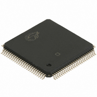
CY7C67300-100AXA Cypress Semiconductor Corp, CY7C67300-100AXA Datasheet - Page 24

CY7C67300-100AXA
Manufacturer Part Number
CY7C67300-100AXA
Description
IC,Peripheral (Multifunction) Controller,QFP,100PIN
Manufacturer
Cypress Semiconductor Corp
Series
EZ-Host™r
Datasheet
1.CY7C67300-100AXA.pdf
(98 pages)
Specifications of CY7C67300-100AXA
Applications
USB Host/Peripheral Controller
Core Processor
CY16
Program Memory Type
ROM (8 kB)
Controller Series
CY7C673xx
Ram Size
16K x 8
Interface
SPI Serial, USB, HPI
Number Of I /o
32
Voltage - Supply
3 V ~ 3.6 V
Operating Temperature
-40°C ~ 85°C
Mounting Type
Surface Mount
Package / Case
100-LQFP
Lead Free Status / RoHS Status
Lead free / RoHS Compliant
For Use With
CY4640 - KIT MASS STORAGE REF DESIGNCY3663 - KIT DEV EZ-OTG/EZ-HOST
Lead Free Status / RoHS Status
Lead free / RoHS Compliant
Available stocks
Company
Part Number
Manufacturer
Quantity
Price
Company:
Part Number:
CY7C67300-100AXA
Manufacturer:
Cypress Semiconductor Corp
Quantity:
10 000
Company:
Part Number:
CY7C67300-100AXAT
Manufacturer:
Cypress Semiconductor Corp
Quantity:
10 000
Document #: 38-08015 Rev. *G
Extended Page n Map Register [R/W]
Register Description
The Extended Page n Map Register contains the Page n high-order address bits. These bits are always appended to accesses
to the Page n Memory mapped space.
Address (Bits [15:0])
The Address field contains the high-order bits 28 to 13 of the Page n address. The address pins [8:0] (Page n address [21:13])
will reflect the content of this register when the CPU accesses the address 0x8000-0x9FFF. For the SRAM mode, the address
pin on [4:0] (Page n address [17:13]) will be used.
Bit [8] (Page n address [21]) should be set to ‘0’, so that Page n reads/writes will access external areas (SRAM, ROM or
peripherals). nXMEMSEL will be the external Chip Select for this space.
Upper Address Enable Register [0xC038] [R/W]
Register Description
The Upper Address Enable Register enables/disables the four
most significant bits of the external address A[18:15]. This
register defaults to having the Upper Address disabled. It
should be noted that on power up pins A[18:15] are driven
high.
Bit #
Field
Read/Write
Default
Bit #
Field
Read/Write
Default
Bit #
Field
Read/Write
Default
Bit #
Field
Read/Write
Default
• Extended Page 1 Map Register 0xC018
• Extended Page 2 Map Register 0xC01A
R/W
R/W
15
15
X
X
0
7
0
7
-
-
R/W
R/W
14
14
X
0
6
0
X
6
-
-
Reserved
Figure 21. External Memory Control Register
Figure 20. Extended Page n Map Register
R/W
R/W
13
13
X
0
5
0
X
5
-
-
R/W
R/W
12
12
0
X
4
0
X
4
-
-
Upper Address Enable (Bit 3)
The Upper Address Enable bit enables/disables the four most
significant bits of the external address A[18:15].
1: Enable A[18:15] of the external memory interface for
general addressing.
0: Disable A[18:15], not available.
Reserved
All reserved bits should be written as ‘0’.
Address...
...Address
Reserved
Address
Enable
Upper
R/W
R/W
R/W
11
11
0
3
0
X
3
0
-
R/W
R/W
10
10
0
X
2
0
X
2
-
Reserved
R/W
R/W
9
0
X
1
0
X
1
9
-
CY7C67300
Page 24 of 98
R/W
R/W
8
0
X
0
0
0
8
X
-
[+] Feedback


