YLCDRSK2378 Renesas Electronics America, YLCDRSK2378 Datasheet - Page 978
YLCDRSK2378
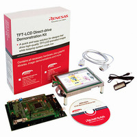
Manufacturer Part Number
YLCDRSK2378
Description
KIT DEV EVAL H8S/2378 LCD
Manufacturer
Renesas Electronics America
Series
H8®r
Datasheet
1.YR0K42378FC000BA.pdf
(1208 pages)
Specifications of YLCDRSK2378
Main Purpose
Displays, LCD Controller
Embedded
Yes, MCU, 16-Bit
Utilized Ic / Part
YLCDRSK2378
Primary Attributes
5.7" QVGA, Touch Screen
Secondary Attributes
Source Code on CD, Debugging Requires Emulator Cable E10A USB/JTAG
Lead Free Status / RoHS Status
Lead free / RoHS Compliant


Section 21 Flash Memory (0.18-μm F-ZTAT Version)
The area that can be executed in the steps of the user procedure program (on-chip RAM, user
MAT, and external space) is shown in section 21.4.4, Procedure Program and Storable Area for
Programming Data.
21.4.4
In the descriptions in the previous section, the programming/erasing procedure programs and
storable areas for program data are assumed to be in the on-chip RAM. However, the program and
the data can be stored in and executed from other areas, such as part of flash memory which is not
to be programmed or erased, or somewhere in the external address space.
(1)
1. The on-chip programming/erasing program is downloaded from the address in the on-chip
2. The on-chip programming/erasing program will use the 128 bytes as a stack. So, make sure
3. Download by setting the SCO bit to 1 will lead to switching of the MAT. If, therefore, this
4. The flash memory is accessible until the start of programming or erasing, that is, until the
5. The flash memory is not accessible during programming/erasing operations, therefore, the
6. After programming/erasing, the flash memory should be inhibited until FKEY is cleared.
7. Switching of the MATs by FMATS should be needed when programming/erasing of the user
Rev.7.00 Mar. 18, 2009 page 910 of 1136
REJ09B0109-0700
RAM specified by FTDAR, therefore, this area is not available for use.
that this area is secured.
operation is used, it should be executed from the on-chip RAM.
result of downloading has been determined. When in a mode in which the external address
space is not accessible, such as single-chip mode, the required procedure programs, NMI
handling vector and NMI handler should be transferred to the on-chip RAM before
programming/erasing of the flash memory starts.
operation program is downloaded to the on-chip RAM to be executed. The NMI-handling
vector and programs such as that which activate the operation program, and NMI handler
should thus be stored in on-chip memory other than flash memory or the external address
space.
The reset state (RES = 0) must be in place for more than 100 μs when the LSI mode is changed
to reset on completion of a programming/erasing operation.
Transitions to the reset state, and hardware standby mode are inhibited during
programming/erasing. When the reset signal is accidentally input to the chip, a longer period in
the reset state than usual (100 μs) is needed before the reset signal is released.
boot MAT is operated in user-boot mode. The program which switches the MATs should be
executed from the on-chip RAM. See section 21.6, Switching between User MAT and User
Conditions that Apply to Programming/Erasing
Procedure Program and Storable Area for Programming Data
Related parts for YLCDRSK2378
Image
Part Number
Description
Manufacturer
Datasheet
Request
R

Part Number:
Description:
KIT STARTER FOR M16C/29
Manufacturer:
Renesas Electronics America
Datasheet:

Part Number:
Description:
KIT STARTER FOR R8C/2D
Manufacturer:
Renesas Electronics America
Datasheet:

Part Number:
Description:
R0K33062P STARTER KIT
Manufacturer:
Renesas Electronics America
Datasheet:

Part Number:
Description:
KIT STARTER FOR R8C/23 E8A
Manufacturer:
Renesas Electronics America
Datasheet:

Part Number:
Description:
KIT STARTER FOR R8C/25
Manufacturer:
Renesas Electronics America
Datasheet:

Part Number:
Description:
KIT STARTER H8S2456 SHARPE DSPLY
Manufacturer:
Renesas Electronics America
Datasheet:

Part Number:
Description:
KIT STARTER FOR R8C38C
Manufacturer:
Renesas Electronics America
Datasheet:

Part Number:
Description:
KIT STARTER FOR R8C35C
Manufacturer:
Renesas Electronics America
Datasheet:

Part Number:
Description:
KIT STARTER FOR R8CL3AC+LCD APPS
Manufacturer:
Renesas Electronics America
Datasheet:
Part Number:
Description:
KIT STARTER FOR RX610
Manufacturer:
Renesas Electronics America
Datasheet:

Part Number:
Description:
KIT STARTER FOR R32C/118
Manufacturer:
Renesas Electronics America
Datasheet:

Part Number:
Description:
KIT DEV RSK-R8C/26-29
Manufacturer:
Renesas Electronics America
Datasheet:

Part Number:
Description:
KIT STARTER FOR SH7124
Manufacturer:
Renesas Electronics America
Datasheet:

Part Number:
Description:
KIT STARTER FOR H8SX/1622
Manufacturer:
Renesas Electronics America
Datasheet:

Part Number:
Description:
KIT DEV FOR SH7203
Manufacturer:
Renesas Electronics America
Datasheet: