YLCDRSK2378 Renesas Electronics America, YLCDRSK2378 Datasheet - Page 48
YLCDRSK2378
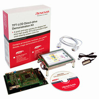
Manufacturer Part Number
YLCDRSK2378
Description
KIT DEV EVAL H8S/2378 LCD
Manufacturer
Renesas Electronics America
Series
H8®r
Datasheet
1.YR0K42378FC000BA.pdf
(1208 pages)
Specifications of YLCDRSK2378
Main Purpose
Displays, LCD Controller
Embedded
Yes, MCU, 16-Bit
Utilized Ic / Part
YLCDRSK2378
Primary Attributes
5.7" QVGA, Touch Screen
Secondary Attributes
Source Code on CD, Debugging Requires Emulator Cable E10A USB/JTAG
Lead Free Status / RoHS Status
Lead free / RoHS Compliant


Figure 6.48 Example of Write Access Timing when CAS Latency Control Cycle Is Disabled
Figure 6.49 DQMU and DQML Control Timing (Upper Byte Write Access:
Figure 6.50 DQMU and DQML Control Timing (Lower Byte Read Access:
Figure 6.51 Example of DQMU and DQML Byte Control ........................................................ 230
Figure 6.52 Operation Timing of Burst Access (BE = 1, SDWCD = 0, CAS Latency 2) ......... 232
Figure 6.53 Example of Operation Timing in RAS Down Mode (BE = 1, CAS Latency 2)..... 234
Figure 6.54 Auto Refresh Timing............................................................................................... 235
Figure 6.55 Auto Refresh Timing (TPC = 1, TPC0 = 1, RCW1 = 0, RCW0 = 1)..................... 236
Figure 6.56 Auto Refresh Timing (TPC = 0, TPC0 = 0, RLW1 = 0, RLW0 = 1) ..................... 237
Figure 6.57 Self-Refresh Timing (TPC1 = 1, TPC0 = 0, RCW1 = 0, RCW0 = 0,
Figure 6.58 Example of Timing when Precharge Time after Self-Refreshing Is Extended
Figure 6.59 Synchronous DRAM Mode Setting Timing............................................................ 240
Figure 6.60 Example of DACK/EDACK Output Timing when DDS = 1 or EDDS = 1 ............ 242
Figure 6.61 Example of DACK/EDACK Output Timing when DDS = 0 or EDDS = 0 ............ 244
Figure 6.62 Example of Timing when the Read Data Is Extended by Two States
Figure 6.63 Example of Burst ROM Access Timing (ASTn = 1, 2-State Burst Cycle) ............. 247
Figure 6.64 Example of Burst ROM Access Timing (ASTn = 0, 1-State Burst Cycle) ............. 248
Figure 6.65 Example of Idle Cycle Operation (Consecutive Reads in Different Areas) ............ 249
Figure 6.66 Example of Idle Cycle Operation (Write after Read) .............................................. 250
Figure 6.67 Example of Idle Cycle Operation (Read after Write) .............................................. 251
Figure 6.68 Relationship between Chip Select (CS) and Read (RD) ......................................... 252
Figure 6.69 Example of DRAM Full Access after External Read (CAST = 0).......................... 253
Figure 6.70 Example of Idle Cycle Operation in RAS Down Mode
Figure 6.71 Example of Idle Cycle Operation in RAS Down Mode (Write after Read)
Figure 6.72 Example of Synchronous DRAM Full Access after External Read
Figure 6.73 Example of Idle Cycle Operation in RAS Down Mode
Figure 6.74 Example of Idle Cycle Operation in RAS Down Mode
Figure 6.75 Example of Idle Cycle Operation in RAS Down Mode
Rev.7.00 Mar. 18, 2009 page xlvi of lxvi
REJ09B0109-0700
(SDWCD = 1) ......................................................................................................... 227
SDWCD = 0, CAS Latency 2) ................................................................................ 228
CAS Latency 2) ....................................................................................................... 229
RLW1 = 0, RLW0 = 0) ........................................................................................... 238
by 2 States (TPCS2 to TPCS0 = H'2, TPC1 = 0, TPC0 = 0, CAS Latency 2) ........ 239
(DDS = 1, or EDDS = 1, RDXC1 = 0, RDXC0 = 1, CAS Latency 2) .................... 245
(Consecutive Reads in Different Areas) (IDLC = 0, RAST = 0, CAST = 0) .......... 254
(IDLC = 0, RAST = 0, CAST = 0).......................................................................... 254
(CAS Latency 2)...................................................................................................... 255
(Read in Different Area) (IDLC = 0, CAS Latency 2) ............................................ 256
(Read in Different Area) (IDLC = 1, CAS Latency 2) ............................................ 257
(Write after Read) (IDLC = 0, CAS Latency 2) ...................................................... 258
Related parts for YLCDRSK2378
Image
Part Number
Description
Manufacturer
Datasheet
Request
R

Part Number:
Description:
KIT STARTER FOR M16C/29
Manufacturer:
Renesas Electronics America
Datasheet:

Part Number:
Description:
KIT STARTER FOR R8C/2D
Manufacturer:
Renesas Electronics America
Datasheet:

Part Number:
Description:
R0K33062P STARTER KIT
Manufacturer:
Renesas Electronics America
Datasheet:

Part Number:
Description:
KIT STARTER FOR R8C/23 E8A
Manufacturer:
Renesas Electronics America
Datasheet:

Part Number:
Description:
KIT STARTER FOR R8C/25
Manufacturer:
Renesas Electronics America
Datasheet:

Part Number:
Description:
KIT STARTER H8S2456 SHARPE DSPLY
Manufacturer:
Renesas Electronics America
Datasheet:

Part Number:
Description:
KIT STARTER FOR R8C38C
Manufacturer:
Renesas Electronics America
Datasheet:

Part Number:
Description:
KIT STARTER FOR R8C35C
Manufacturer:
Renesas Electronics America
Datasheet:

Part Number:
Description:
KIT STARTER FOR R8CL3AC+LCD APPS
Manufacturer:
Renesas Electronics America
Datasheet:
Part Number:
Description:
KIT STARTER FOR RX610
Manufacturer:
Renesas Electronics America
Datasheet:

Part Number:
Description:
KIT STARTER FOR R32C/118
Manufacturer:
Renesas Electronics America
Datasheet:

Part Number:
Description:
KIT DEV RSK-R8C/26-29
Manufacturer:
Renesas Electronics America
Datasheet:

Part Number:
Description:
KIT STARTER FOR SH7124
Manufacturer:
Renesas Electronics America
Datasheet:

Part Number:
Description:
KIT STARTER FOR H8SX/1622
Manufacturer:
Renesas Electronics America
Datasheet:

Part Number:
Description:
KIT DEV FOR SH7203
Manufacturer:
Renesas Electronics America
Datasheet: