YLCDRSK2378 Renesas Electronics America, YLCDRSK2378 Datasheet - Page 603
YLCDRSK2378
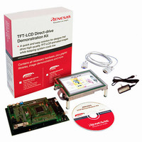
Manufacturer Part Number
YLCDRSK2378
Description
KIT DEV EVAL H8S/2378 LCD
Manufacturer
Renesas Electronics America
Series
H8®r
Datasheet
1.YR0K42378FC000BA.pdf
(1208 pages)
Specifications of YLCDRSK2378
Main Purpose
Displays, LCD Controller
Embedded
Yes, MCU, 16-Bit
Utilized Ic / Part
YLCDRSK2378
Primary Attributes
5.7" QVGA, Touch Screen
Secondary Attributes
Source Code on CD, Debugging Requires Emulator Cable E10A USB/JTAG
Lead Free Status / RoHS Status
Lead free / RoHS Compliant


10.15
Port G is a 7-bit I/O port that also has other functions. The port G has the following registers.
• Port G data direction register (PGDDR)
• Port G data register (PGDR)
• Port G register (PORTG)
• Port Function Control Register 0 (PFCR0)
10.15.1 Port G Data Direction Register (PGDDR)
The individual bits of PGDDR specify input or output for the pins of port G.
PGDDR cannot be read; if it is, an undefined value will be read.
Bit
7
6
5
4
3
2
1
0
Note:
Bit Name
⎯
PG6DDR
PG5DDR
PG4DDR
PG3DDR
PG2DDR
PG1DDR
PG0DDR
* PG0DDR is initialized to 1 in modes 1 and 2, and to 0 in modes 4 and 7.
Port G
Initial Value
0
0
0
0
0
0
0
1/0 *
R/W
⎯
W
W
W
W
W
W
W
Description
Reserved
•
•
Modes 7 (when EXPE = 1), 1, 2, and 4
Pins PG6 to PG4 function as bus control
input/output pins (BREQO, BACK, and BREQ)
when the appropriate bus controller settings are
made. Otherwise, these pins are I/O ports, and their
functions can be switched with PGDDR.
When the CS output enable bits (CS3E to CS0E)
are set to 1, pins PG3 to PG0 function as CS output
pins when the corresponding PGDDR bit is set to 1,
and as input ports when the bit is cleared to 0.
When CS3E to CS0E are cleared to 0, pins PG3 to
PG0 are I/O ports, and their functions can be
switched with PGDDR.
Mode 7 (when EXPE = 0)
Pins PG6 to PG0 are I/O ports, and their functions
can be switched with PGDDR.
Rev.7.00 Mar. 18, 2009 page 535 of 1136
Section 10 I/O Ports
REJ09B0109-0700
Related parts for YLCDRSK2378
Image
Part Number
Description
Manufacturer
Datasheet
Request
R

Part Number:
Description:
KIT STARTER FOR M16C/29
Manufacturer:
Renesas Electronics America
Datasheet:

Part Number:
Description:
KIT STARTER FOR R8C/2D
Manufacturer:
Renesas Electronics America
Datasheet:

Part Number:
Description:
R0K33062P STARTER KIT
Manufacturer:
Renesas Electronics America
Datasheet:

Part Number:
Description:
KIT STARTER FOR R8C/23 E8A
Manufacturer:
Renesas Electronics America
Datasheet:

Part Number:
Description:
KIT STARTER FOR R8C/25
Manufacturer:
Renesas Electronics America
Datasheet:

Part Number:
Description:
KIT STARTER H8S2456 SHARPE DSPLY
Manufacturer:
Renesas Electronics America
Datasheet:

Part Number:
Description:
KIT STARTER FOR R8C38C
Manufacturer:
Renesas Electronics America
Datasheet:

Part Number:
Description:
KIT STARTER FOR R8C35C
Manufacturer:
Renesas Electronics America
Datasheet:

Part Number:
Description:
KIT STARTER FOR R8CL3AC+LCD APPS
Manufacturer:
Renesas Electronics America
Datasheet:
Part Number:
Description:
KIT STARTER FOR RX610
Manufacturer:
Renesas Electronics America
Datasheet:

Part Number:
Description:
KIT STARTER FOR R32C/118
Manufacturer:
Renesas Electronics America
Datasheet:

Part Number:
Description:
KIT DEV RSK-R8C/26-29
Manufacturer:
Renesas Electronics America
Datasheet:

Part Number:
Description:
KIT STARTER FOR SH7124
Manufacturer:
Renesas Electronics America
Datasheet:

Part Number:
Description:
KIT STARTER FOR H8SX/1622
Manufacturer:
Renesas Electronics America
Datasheet:

Part Number:
Description:
KIT DEV FOR SH7203
Manufacturer:
Renesas Electronics America
Datasheet: