YLCDRSK2378 Renesas Electronics America, YLCDRSK2378 Datasheet - Page 947
YLCDRSK2378
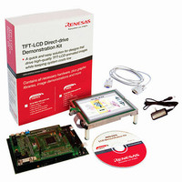
Manufacturer Part Number
YLCDRSK2378
Description
KIT DEV EVAL H8S/2378 LCD
Manufacturer
Renesas Electronics America
Series
H8®r
Datasheet
1.YR0K42378FC000BA.pdf
(1208 pages)
Specifications of YLCDRSK2378
Main Purpose
Displays, LCD Controller
Embedded
Yes, MCU, 16-Bit
Utilized Ic / Part
YLCDRSK2378
Primary Attributes
5.7" QVGA, Touch Screen
Secondary Attributes
Source Code on CD, Debugging Requires Emulator Cable E10A USB/JTAG
Lead Free Status / RoHS Status
Lead free / RoHS Compliant


Section 21 Flash Memory (0.18-μm F-ZTAT Version)
21.3.2
Programming/Erasing Interface Parameter
The programming/erasing interface parameter specifies the operating frequency, storage place for
program data, programming destination address, and erase block and exchanges the processing
result for the downloaded on-chip program. This parameter uses the general registers of the CPU
(ER0 and ER1) or the on-chip RAM area. The initial value is undefined at a power-on reset or in
hardware standby mode.
When download, initialization, or on-chip program is executed, registers of the CPU except for
ER0 and ER1 are stored. The return value of the processing result is written in ER0, ER1. Since
the stack area is used for storing the registers except for ER0, ER1, the stack area must be saved at
the processing start. (A maximum size of a stack area to be used is 128 bytes.)
The programming/erasing interface parameter is used in the following four items.
1. Download control
2. Initialization before programming or erasing
3. Programming
4. Erasing
These items use different parameters. The correspondence table is shown in table 21.4. The
meaning of the bits in FPFR varies in each processing program: initialization, programming, or
erasure. For details, see descriptions of FPFR for each process.
Rev.7.00 Mar. 18, 2009 page 879 of 1136
REJ09B0109-0700
Related parts for YLCDRSK2378
Image
Part Number
Description
Manufacturer
Datasheet
Request
R

Part Number:
Description:
KIT STARTER FOR M16C/29
Manufacturer:
Renesas Electronics America
Datasheet:

Part Number:
Description:
KIT STARTER FOR R8C/2D
Manufacturer:
Renesas Electronics America
Datasheet:

Part Number:
Description:
R0K33062P STARTER KIT
Manufacturer:
Renesas Electronics America
Datasheet:

Part Number:
Description:
KIT STARTER FOR R8C/23 E8A
Manufacturer:
Renesas Electronics America
Datasheet:

Part Number:
Description:
KIT STARTER FOR R8C/25
Manufacturer:
Renesas Electronics America
Datasheet:

Part Number:
Description:
KIT STARTER H8S2456 SHARPE DSPLY
Manufacturer:
Renesas Electronics America
Datasheet:

Part Number:
Description:
KIT STARTER FOR R8C38C
Manufacturer:
Renesas Electronics America
Datasheet:

Part Number:
Description:
KIT STARTER FOR R8C35C
Manufacturer:
Renesas Electronics America
Datasheet:

Part Number:
Description:
KIT STARTER FOR R8CL3AC+LCD APPS
Manufacturer:
Renesas Electronics America
Datasheet:
Part Number:
Description:
KIT STARTER FOR RX610
Manufacturer:
Renesas Electronics America
Datasheet:

Part Number:
Description:
KIT STARTER FOR R32C/118
Manufacturer:
Renesas Electronics America
Datasheet:

Part Number:
Description:
KIT DEV RSK-R8C/26-29
Manufacturer:
Renesas Electronics America
Datasheet:

Part Number:
Description:
KIT STARTER FOR SH7124
Manufacturer:
Renesas Electronics America
Datasheet:

Part Number:
Description:
KIT STARTER FOR H8SX/1622
Manufacturer:
Renesas Electronics America
Datasheet:

Part Number:
Description:
KIT DEV FOR SH7203
Manufacturer:
Renesas Electronics America
Datasheet: