YLCDRSK2378 Renesas Electronics America, YLCDRSK2378 Datasheet - Page 224
YLCDRSK2378
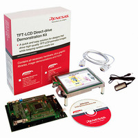
Manufacturer Part Number
YLCDRSK2378
Description
KIT DEV EVAL H8S/2378 LCD
Manufacturer
Renesas Electronics America
Series
H8®r
Datasheet
1.YR0K42378FC000BA.pdf
(1208 pages)
Specifications of YLCDRSK2378
Main Purpose
Displays, LCD Controller
Embedded
Yes, MCU, 16-Bit
Utilized Ic / Part
YLCDRSK2378
Primary Attributes
5.7" QVGA, Touch Screen
Secondary Attributes
Source Code on CD, Debugging Requires Emulator Cable E10A USB/JTAG
Lead Free Status / RoHS Status
Lead free / RoHS Compliant


Section 6 Bus Controller (BSC)
6.3.8
DRAMCR is used to make DRAM/synchronous DRAM interface settings.
Note: The synchronous DRAM interface is not supported by the H8S/2378 Group.
Bit
15
14
13
Rev.7.00 Mar. 18, 2009 page 156 of 1136
REJ09B0109-0700
Bit Name
OEE
RAST
—
DRAM Control Register (DRAMCR)
Initial Value
0
0
0
R/W
R/W
R/W
R/W
Description
OE Output Enable
The OE signal used when EDO page mode DRAM
is connected can be output from the (OE) pin. The
OE signal is common to all areas designated as
DRAM space.
When the synchronous DRAM is connected, the
CKE signal can be output from the (OE) pin. The
CKE signal is common to the continuous
synchronous DRAM space.
0: OE/CKE signal output disabled
1: OE/CKE signal output enabled
RAS Assertion Timing Select
Selects whether, in DRAM access, the RAS signal
is asserted from the start of the T
edge of φ) or from the falling edge of φ.
Figure 6.4 shows the relationship between the
RAST bit setting and the RAS assertion timing.
The setting of this bit applies to all areas
designated as DRAM space.
0: RAS is asserted from φ falling edge in T
1: RAS is asserted from start of T
Reserved
This bit can be read from or written to. However,
the write value should always be 0.
(OE)/(CKE) pin can be used as I/O port
r
r
cycle (rising
cycle
r
cycle
Related parts for YLCDRSK2378
Image
Part Number
Description
Manufacturer
Datasheet
Request
R

Part Number:
Description:
KIT STARTER FOR M16C/29
Manufacturer:
Renesas Electronics America
Datasheet:

Part Number:
Description:
KIT STARTER FOR R8C/2D
Manufacturer:
Renesas Electronics America
Datasheet:

Part Number:
Description:
R0K33062P STARTER KIT
Manufacturer:
Renesas Electronics America
Datasheet:

Part Number:
Description:
KIT STARTER FOR R8C/23 E8A
Manufacturer:
Renesas Electronics America
Datasheet:

Part Number:
Description:
KIT STARTER FOR R8C/25
Manufacturer:
Renesas Electronics America
Datasheet:

Part Number:
Description:
KIT STARTER H8S2456 SHARPE DSPLY
Manufacturer:
Renesas Electronics America
Datasheet:

Part Number:
Description:
KIT STARTER FOR R8C38C
Manufacturer:
Renesas Electronics America
Datasheet:

Part Number:
Description:
KIT STARTER FOR R8C35C
Manufacturer:
Renesas Electronics America
Datasheet:

Part Number:
Description:
KIT STARTER FOR R8CL3AC+LCD APPS
Manufacturer:
Renesas Electronics America
Datasheet:
Part Number:
Description:
KIT STARTER FOR RX610
Manufacturer:
Renesas Electronics America
Datasheet:

Part Number:
Description:
KIT STARTER FOR R32C/118
Manufacturer:
Renesas Electronics America
Datasheet:

Part Number:
Description:
KIT DEV RSK-R8C/26-29
Manufacturer:
Renesas Electronics America
Datasheet:

Part Number:
Description:
KIT STARTER FOR SH7124
Manufacturer:
Renesas Electronics America
Datasheet:

Part Number:
Description:
KIT STARTER FOR H8SX/1622
Manufacturer:
Renesas Electronics America
Datasheet:

Part Number:
Description:
KIT DEV FOR SH7203
Manufacturer:
Renesas Electronics America
Datasheet: