YLCDRSK2378 Renesas Electronics America, YLCDRSK2378 Datasheet - Page 809
YLCDRSK2378
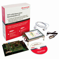
Manufacturer Part Number
YLCDRSK2378
Description
KIT DEV EVAL H8S/2378 LCD
Manufacturer
Renesas Electronics America
Series
H8®r
Datasheet
1.YR0K42378FC000BA.pdf
(1208 pages)
Specifications of YLCDRSK2378
Main Purpose
Displays, LCD Controller
Embedded
Yes, MCU, 16-Bit
Utilized Ic / Part
YLCDRSK2378
Primary Attributes
5.7" QVGA, Touch Screen
Secondary Attributes
Source Code on CD, Debugging Requires Emulator Cable E10A USB/JTAG
Lead Free Status / RoHS Status
Lead free / RoHS Compliant


15.6.2
Before transmitting and receiving data, you should first clear the TE and RE bits in SCR to 0, then
initialize the SCI as described in a sample flowchart in figure 15.15. Do not write to SMR, SCMR,
IrCR, or SEMR while the SCI is operating. This also applies to writing the same data as the
current register contents. When the operating mode, transfer format, etc., is changed, the TE and
RE bits must be cleared to 0 before making the change. When the TE bit is cleared to 0, the TDRE
flag is set to 1. Note that clearing the RE bit to 0 does not change the contents of the RDRF, PER,
FER, and ORER flags, or the contents of RDR.
15.6.3
Figure 15.16 shows an example of SCI operation for transmission in clocked synchronous mode.
In serial transmission, the SCI operates as described below.
SCI Initialization (Clocked Synchronous Mode)
Serial Data Transmission (Clocked Synchronous Mode)
Note: In simultaneous transmit and receive operations, the TE and RE bits should
Set TE and RE bits in SCR to 1, and
set RIE, TIE, TEIE, and MPIE bits
Clear TE and RE bits in SCR to 0
Set CKE1 and CKE0 bits in SCR
Set data transfer format in
both be cleared to 0 or set to 1 simultaneously.
1-bit interval elapsed?
Start of initialization
Set value in BRR
SMR and SCMR
<Transfer start>
(TE, RE bits 0)
Figure 15.15 Sample SCI Initialization Flowchart
Yes
Wait
No
Section 15 Serial Communication Interface (SCI, IrDA)
[4]
[2]
[3]
[1]
[1] Set the clock selection in SCR. Be sure
[2] Set the data transfer format in SMR
[3] Write a value corresponding to the bit
[4] Wait at least one bit interval, then set
to clear bits RIE, TIE, TEIE, and MPIE,
TE and RE, to 0.
and SCMR.
rate to BRR. (Not necessary if an
external clock is used.)
the TE and RE bits in SCR to 1.
Also set the RIE, TIE, TEIE, and MPIE
bits.
Setting the TE and RE bits enable the
TxD and RxD pins to be used.
Rev.7.00 Mar. 18, 2009 page 741 of 1136
REJ09B0109-0700
Related parts for YLCDRSK2378
Image
Part Number
Description
Manufacturer
Datasheet
Request
R

Part Number:
Description:
KIT STARTER FOR M16C/29
Manufacturer:
Renesas Electronics America
Datasheet:

Part Number:
Description:
KIT STARTER FOR R8C/2D
Manufacturer:
Renesas Electronics America
Datasheet:

Part Number:
Description:
R0K33062P STARTER KIT
Manufacturer:
Renesas Electronics America
Datasheet:

Part Number:
Description:
KIT STARTER FOR R8C/23 E8A
Manufacturer:
Renesas Electronics America
Datasheet:

Part Number:
Description:
KIT STARTER FOR R8C/25
Manufacturer:
Renesas Electronics America
Datasheet:

Part Number:
Description:
KIT STARTER H8S2456 SHARPE DSPLY
Manufacturer:
Renesas Electronics America
Datasheet:

Part Number:
Description:
KIT STARTER FOR R8C38C
Manufacturer:
Renesas Electronics America
Datasheet:

Part Number:
Description:
KIT STARTER FOR R8C35C
Manufacturer:
Renesas Electronics America
Datasheet:

Part Number:
Description:
KIT STARTER FOR R8CL3AC+LCD APPS
Manufacturer:
Renesas Electronics America
Datasheet:
Part Number:
Description:
KIT STARTER FOR RX610
Manufacturer:
Renesas Electronics America
Datasheet:

Part Number:
Description:
KIT STARTER FOR R32C/118
Manufacturer:
Renesas Electronics America
Datasheet:

Part Number:
Description:
KIT DEV RSK-R8C/26-29
Manufacturer:
Renesas Electronics America
Datasheet:

Part Number:
Description:
KIT STARTER FOR SH7124
Manufacturer:
Renesas Electronics America
Datasheet:

Part Number:
Description:
KIT STARTER FOR H8SX/1622
Manufacturer:
Renesas Electronics America
Datasheet:

Part Number:
Description:
KIT DEV FOR SH7203
Manufacturer:
Renesas Electronics America
Datasheet: