YLCDRSK2378 Renesas Electronics America, YLCDRSK2378 Datasheet - Page 57
YLCDRSK2378
Manufacturer Part Number
YLCDRSK2378
Description
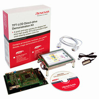
KIT DEV EVAL H8S/2378 LCD
Manufacturer
Renesas Electronics America
Series
H8®r
Datasheet
1.YR0K42378FC000BA.pdf
(1208 pages)
Specifications of YLCDRSK2378
Main Purpose
Displays, LCD Controller
Embedded
Yes, MCU, 16-Bit
Utilized Ic / Part
YLCDRSK2378
Primary Attributes
5.7" QVGA, Touch Screen
Secondary Attributes
Source Code on CD, Debugging Requires Emulator Cable E10A USB/JTAG
Lead Free Status / RoHS Status
Lead free / RoHS Compliant


Figure 18.2 Block Diagram of D/A Converter for H8S/2375, H8S/2375R, H8S/2373,
Figure 18.3 Example of D/A Converter Operation..................................................................... 830
Section 20 Flash Memory (0.35-μm F-ZTAT Version) ....................................833
Figure 20.1 Block Diagram of Flash Memory........................................................................... 834
Figure 20.2 Flash Memory State Transitions.............................................................................. 835
Figure 20.3 Boot Mode............................................................................................................... 836
Figure 20.4 User Program Mode ................................................................................................ 837
Figure 20.5 384-kbyte Flash Memory Block Configuration (Modes 3, 4, and 7)....................... 839
Figure 20.6 Programming/Erasing Flowchart Example in User Program Mode ........................ 849
Figure 20.7 Program/Program-Verify Flowchart ....................................................................... 851
Figure 20.8 Erase/Erase-Verify Flowchart ................................................................................. 853
Figure 20.9 Power-On/Off Timing ............................................................................................. 858
Figure 20.10 Mode Transition Timing
Section 21 Flash Memory (0.18-μm F-ZTAT Version) ....................................861
Figure 21.1 Block Diagram of Flash Memory............................................................................ 863
Figure 21.2 Mode Transition of Flash Memory.......................................................................... 864
Figure 21.3 Flash Memory Configuration .................................................................................. 866
Figure 21.4 Block Division of User MAT .................................................................................. 867
Figure 21.5 Overview of User Procedure Program .................................................................... 868
Figure 21.6 System Configuration in Boot Mode....................................................................... 892
Figure 21.7 Automatic-Bit-Rate Adjustment Operation of SCI ................................................. 892
Figure 21.8 Overview of Boot Mode State Transition Diagram................................................. 894
Figure 21.9 Programming/Erasing Overview Flow.................................................................... 895
Figure 21.10 RAM Map when Programming/Erasing Is Executed .............................................. 896
Figure 21.11 Programming Procedure.......................................................................................... 897
Figure 21.12 Erasing Procedure ................................................................................................... 904
Figure 21.13 Procedure for Programming User MAT in User Boot Mode .................................. 907
Figure 21.14 Procedure for Erasing User MAT in User Boot Mode ............................................ 909
Figure 21.15 Transitions to Error-Protection State....................................................................... 922
Figure 21.16 Switching between the User MAT and User Boot MAT ........................................ 923
Figure 21.17 Boot Program States................................................................................................ 925
Figure 21.18 Bit-Rate-Adjustment Sequence ............................................................................... 926
Figure 21.19 Communication Protocol Format ............................................................................ 927
Figure 21.20 New Bit-Rate Selection Sequence........................................................................... 938
Figure 21.21 Programming Sequence........................................................................................... 942
Figure 21.22 Erasure Sequence .................................................................................................... 945
and H8S/2373R ....................................................................................................... 823
(Example: Boot Mode → User Mode ↔ User Program Mode).............................. 859
Rev.7.00 Mar. 18, 2009 page lv of lxvi
REJ09B0109-0700
Related parts for YLCDRSK2378
Image
Part Number
Description
Manufacturer
Datasheet
Request
R

Part Number:
Description:
KIT STARTER FOR M16C/29
Manufacturer:
Renesas Electronics America
Datasheet:

Part Number:
Description:
KIT STARTER FOR R8C/2D
Manufacturer:
Renesas Electronics America
Datasheet:

Part Number:
Description:
R0K33062P STARTER KIT
Manufacturer:
Renesas Electronics America
Datasheet:

Part Number:
Description:
KIT STARTER FOR R8C/23 E8A
Manufacturer:
Renesas Electronics America
Datasheet:

Part Number:
Description:
KIT STARTER FOR R8C/25
Manufacturer:
Renesas Electronics America
Datasheet:

Part Number:
Description:
KIT STARTER H8S2456 SHARPE DSPLY
Manufacturer:
Renesas Electronics America
Datasheet:

Part Number:
Description:
KIT STARTER FOR R8C38C
Manufacturer:
Renesas Electronics America
Datasheet:

Part Number:
Description:
KIT STARTER FOR R8C35C
Manufacturer:
Renesas Electronics America
Datasheet:

Part Number:
Description:
KIT STARTER FOR R8CL3AC+LCD APPS
Manufacturer:
Renesas Electronics America
Datasheet:
Part Number:
Description:
KIT STARTER FOR RX610
Manufacturer:
Renesas Electronics America
Datasheet:

Part Number:
Description:
KIT STARTER FOR R32C/118
Manufacturer:
Renesas Electronics America
Datasheet:

Part Number:
Description:
KIT DEV RSK-R8C/26-29
Manufacturer:
Renesas Electronics America
Datasheet:

Part Number:
Description:
KIT STARTER FOR SH7124
Manufacturer:
Renesas Electronics America
Datasheet:

Part Number:
Description:
KIT STARTER FOR H8SX/1622
Manufacturer:
Renesas Electronics America
Datasheet:

Part Number:
Description:
KIT DEV FOR SH7203
Manufacturer:
Renesas Electronics America
Datasheet: