YLCDRSK2378 Renesas Electronics America, YLCDRSK2378 Datasheet - Page 273
YLCDRSK2378
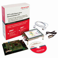
Manufacturer Part Number
YLCDRSK2378
Description
KIT DEV EVAL H8S/2378 LCD
Manufacturer
Renesas Electronics America
Series
H8®r
Datasheet
1.YR0K42378FC000BA.pdf
(1208 pages)
Specifications of YLCDRSK2378
Main Purpose
Displays, LCD Controller
Embedded
Yes, MCU, 16-Bit
Utilized Ic / Part
YLCDRSK2378
Primary Attributes
5.7" QVGA, Touch Screen
Secondary Attributes
Source Code on CD, Debugging Requires Emulator Cable E10A USB/JTAG
Lead Free Status / RoHS Status
Lead free / RoHS Compliant


The bus cycle can also be extended in burst access by inserting wait states. The wait state insertion
method and timing are the same as for full access. For details see section 6.6.9, Wait Control.
RAS Down Mode and RAS Up Mode: Even when burst operation is selected, it may happen that
access to DRAM space is not continuous, but is interrupted by access to another space. In this
case, if the RAS signal is held low during the access to the other space, burst operation can be
resumed when the same row address in DRAM space is accessed again.
• RAS Down Mode
Note: n = 2 to 5
Read
Write
To select RAS down mode, set both the RCDM bit and the BE bit to 1 in DRAMCR. If access
to DRAM space is interrupted and another space is accessed, the RAS signal is held low
during the access to the other space, and burst access is performed when the row address of the
next DRAM space access is the same as the row address of the previous DRAM space access.
Figure 6.32 shows an example of the timing in RAS down mode.
Note, however, that the RAS signal will go high if:
φ
Address bus
RASn (CSn)
UCAS, LCAS
WE (HWR)
OE (RD)
Data bus
WE (HWR)
OE (RD)
Data bus
Figure 6.31 Operation Timing in Fast Page Mode
T
Row address
p
T
r
(RAST = 0, CAST = 1)
High
High
T
c1
Column address 1
T
c2
Rev.7.00 Mar. 18, 2009 page 205 of 1136
T
c3
Section 6 Bus Controller (BSC)
T
c1
Column address 2
REJ09B0109-0700
T
c2
T
c3
Related parts for YLCDRSK2378
Image
Part Number
Description
Manufacturer
Datasheet
Request
R

Part Number:
Description:
KIT STARTER FOR M16C/29
Manufacturer:
Renesas Electronics America
Datasheet:

Part Number:
Description:
KIT STARTER FOR R8C/2D
Manufacturer:
Renesas Electronics America
Datasheet:

Part Number:
Description:
R0K33062P STARTER KIT
Manufacturer:
Renesas Electronics America
Datasheet:

Part Number:
Description:
KIT STARTER FOR R8C/23 E8A
Manufacturer:
Renesas Electronics America
Datasheet:

Part Number:
Description:
KIT STARTER FOR R8C/25
Manufacturer:
Renesas Electronics America
Datasheet:

Part Number:
Description:
KIT STARTER H8S2456 SHARPE DSPLY
Manufacturer:
Renesas Electronics America
Datasheet:

Part Number:
Description:
KIT STARTER FOR R8C38C
Manufacturer:
Renesas Electronics America
Datasheet:

Part Number:
Description:
KIT STARTER FOR R8C35C
Manufacturer:
Renesas Electronics America
Datasheet:

Part Number:
Description:
KIT STARTER FOR R8CL3AC+LCD APPS
Manufacturer:
Renesas Electronics America
Datasheet:
Part Number:
Description:
KIT STARTER FOR RX610
Manufacturer:
Renesas Electronics America
Datasheet:

Part Number:
Description:
KIT STARTER FOR R32C/118
Manufacturer:
Renesas Electronics America
Datasheet:

Part Number:
Description:
KIT DEV RSK-R8C/26-29
Manufacturer:
Renesas Electronics America
Datasheet:

Part Number:
Description:
KIT STARTER FOR SH7124
Manufacturer:
Renesas Electronics America
Datasheet:

Part Number:
Description:
KIT STARTER FOR H8SX/1622
Manufacturer:
Renesas Electronics America
Datasheet:

Part Number:
Description:
KIT DEV FOR SH7203
Manufacturer:
Renesas Electronics America
Datasheet: