YLCDRSK2378 Renesas Electronics America, YLCDRSK2378 Datasheet - Page 862
YLCDRSK2378
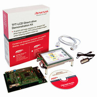
Manufacturer Part Number
YLCDRSK2378
Description
KIT DEV EVAL H8S/2378 LCD
Manufacturer
Renesas Electronics America
Series
H8®r
Datasheet
1.YR0K42378FC000BA.pdf
(1208 pages)
Specifications of YLCDRSK2378
Main Purpose
Displays, LCD Controller
Embedded
Yes, MCU, 16-Bit
Utilized Ic / Part
YLCDRSK2378
Primary Attributes
5.7" QVGA, Touch Screen
Secondary Attributes
Source Code on CD, Debugging Requires Emulator Cable E10A USB/JTAG
Lead Free Status / RoHS Status
Lead free / RoHS Compliant


Section 16 I
16.4.5
In slave receive mode, the master device outputs the transmit clock and transmit data, and the
slave device returns an acknowledge signal. The reception procedure and operations in slave
receive mode are described below.
1. Set the ICE bit in ICCRA to 1. Set the MLS and WAIT bits in ICMR and the CKS3 to CKS0
2. When the slave address matches in the first frame following detection of the start condition,
3. Clear RDRF after reading ICDRR every time RDRF is set. If 8th receive clock pulse falls
4. The last byte data is read by reading ICDRR.
Rev.7.00 Mar. 18, 2009 page 794 of 1136
REJ09B0109-0700
bits in ICCRA to 1. (Initial setting) Set the MST and TRS bits in ICCRA to select slave receive
mode, and wait until the slave address matches.
the slave device outputs the level specified by ACKBT in ICIER to SDA, at the rise of the 9th
clock pulse. At the same time, RDRF in ICSR is set to read ICDRR (dummy read) and RDRF
is cleared. (Since the read data show the slave address and R/W, it is not used.)
while RDRF is 1, SCL is fixed low until ICDRR is read. The change of the acknowledge
before reading ICDRR, to be returned to the master device, is reflected to the next transmit
frame.
Slave Receive Operation
2
C Bus Interface 2 (IIC2) (Option)
Related parts for YLCDRSK2378
Image
Part Number
Description
Manufacturer
Datasheet
Request
R

Part Number:
Description:
KIT STARTER FOR M16C/29
Manufacturer:
Renesas Electronics America
Datasheet:

Part Number:
Description:
KIT STARTER FOR R8C/2D
Manufacturer:
Renesas Electronics America
Datasheet:

Part Number:
Description:
R0K33062P STARTER KIT
Manufacturer:
Renesas Electronics America
Datasheet:

Part Number:
Description:
KIT STARTER FOR R8C/23 E8A
Manufacturer:
Renesas Electronics America
Datasheet:

Part Number:
Description:
KIT STARTER FOR R8C/25
Manufacturer:
Renesas Electronics America
Datasheet:

Part Number:
Description:
KIT STARTER H8S2456 SHARPE DSPLY
Manufacturer:
Renesas Electronics America
Datasheet:

Part Number:
Description:
KIT STARTER FOR R8C38C
Manufacturer:
Renesas Electronics America
Datasheet:

Part Number:
Description:
KIT STARTER FOR R8C35C
Manufacturer:
Renesas Electronics America
Datasheet:

Part Number:
Description:
KIT STARTER FOR R8CL3AC+LCD APPS
Manufacturer:
Renesas Electronics America
Datasheet:
Part Number:
Description:
KIT STARTER FOR RX610
Manufacturer:
Renesas Electronics America
Datasheet:

Part Number:
Description:
KIT STARTER FOR R32C/118
Manufacturer:
Renesas Electronics America
Datasheet:

Part Number:
Description:
KIT DEV RSK-R8C/26-29
Manufacturer:
Renesas Electronics America
Datasheet:

Part Number:
Description:
KIT STARTER FOR SH7124
Manufacturer:
Renesas Electronics America
Datasheet:

Part Number:
Description:
KIT STARTER FOR H8SX/1622
Manufacturer:
Renesas Electronics America
Datasheet:

Part Number:
Description:
KIT DEV FOR SH7203
Manufacturer:
Renesas Electronics America
Datasheet: