YLCDRSK2378 Renesas Electronics America, YLCDRSK2378 Datasheet - Page 53
YLCDRSK2378
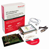
Manufacturer Part Number
YLCDRSK2378
Description
KIT DEV EVAL H8S/2378 LCD
Manufacturer
Renesas Electronics America
Series
H8®r
Datasheet
1.YR0K42378FC000BA.pdf
(1208 pages)
Specifications of YLCDRSK2378
Main Purpose
Displays, LCD Controller
Embedded
Yes, MCU, 16-Bit
Utilized Ic / Part
YLCDRSK2378
Primary Attributes
5.7" QVGA, Touch Screen
Secondary Attributes
Source Code on CD, Debugging Requires Emulator Cable E10A USB/JTAG
Lead Free Status / RoHS Status
Lead free / RoHS Compliant


Figure 11.11 Example of Synchronous Operation........................................................................ 591
Figure 11.12 Compare Match Buffer Operation........................................................................... 592
Figure 11.13 Input Capture Buffer Operation............................................................................... 592
Figure 11.14 Example of Buffer Operation Setting Procedure..................................................... 593
Figure 11.15 Example of Buffer Operation (1) ............................................................................ 594
Figure 11.16 Example of Buffer Operation (2) ............................................................................ 595
Figure 11.17 Cascaded Operation Setting Procedure ................................................................... 596
Figure 11.18 Example of Cascaded Operation (1)........................................................................ 597
Figure 11.19 Example of Cascaded Operation (2)........................................................................ 597
Figure 11.20 Example of PWM Mode Setting Procedure ............................................................ 600
Figure 11.21 Example of PWM Mode Operation (1) ................................................................... 601
Figure 11.22 Example of PWM Mode Operation (2) ................................................................... 601
Figure 11.23 Example of PWM Mode Operation (3) ................................................................... 602
Figure 11.24 Example of Phase Counting Mode Setting Procedure............................................. 603
Figure 11.25 Example of Phase Counting Mode 1 Operation ...................................................... 604
Figure 11.26 Example of Phase Counting Mode 2 Operation ...................................................... 605
Figure 11.27 Example of Phase Counting Mode 3 Operation ...................................................... 606
Figure 11.28 Example of Phase Counting Mode 4 Operation ...................................................... 607
Figure 11.29 Phase Counting Mode Application Example........................................................... 609
Figure 11.30 Count Timing in Internal Clock Operation.............................................................. 612
Figure 11.31 Count Timing in External Clock Operation ............................................................ 612
Figure 11.32 Output Compare Output Timing ............................................................................. 613
Figure 11.33 Input Capture Input Signal Timing.......................................................................... 613
Figure 11.34 Counter Clear Timing (Compare Match) ................................................................ 614
Figure 11.35 Counter Clear Timing (Input Capture) .................................................................... 614
Figure 11.36 Buffer Operation Timing (Compare Match) ........................................................... 615
Figure 11.37 Buffer Operation Timing (Input Capture) ............................................................... 615
Figure 11.38 TGI Interrupt Timing (Compare Match) ................................................................. 616
Figure 11.39 TGI Interrupt Timing (Input Capture) ..................................................................... 616
Figure 11.40 TCIV Interrupt Setting Timing................................................................................ 617
Figure 11.41 TCIU Interrupt Setting Timing................................................................................ 617
Figure 11.42 Timing for Status Flag Clearing by CPU ................................................................ 618
Figure 11.43 Timing for Status Flag Clearing by DTC/DMAC Activation ................................. 618
Figure 11.44 Phase Difference, Overlap, and Pulse Width in Phase Counting Mode .................. 619
Figure 11.45 Contention between TCNT Write and Clear Operations......................................... 620
Figure 11.46 Contention between TCNT Write and Increment Operations ................................. 621
Figure 11.47 Contention between TGR Write and Compare Match ............................................ 622
Figure 11.48 Contention between Buffer Register Write and Compare Match............................ 623
Figure 11.49 Contention between TGR Read and Input Capture ................................................. 624
Figure 11.50 Contention between TGR Write and Input Capture ................................................ 625
Figure 11.51 Contention between Buffer Register Write and Input Capture................................ 626
Rev.7.00 Mar. 18, 2009 page li of lxvi
REJ09B0109-0700
Related parts for YLCDRSK2378
Image
Part Number
Description
Manufacturer
Datasheet
Request
R

Part Number:
Description:
KIT STARTER FOR M16C/29
Manufacturer:
Renesas Electronics America
Datasheet:

Part Number:
Description:
KIT STARTER FOR R8C/2D
Manufacturer:
Renesas Electronics America
Datasheet:

Part Number:
Description:
R0K33062P STARTER KIT
Manufacturer:
Renesas Electronics America
Datasheet:

Part Number:
Description:
KIT STARTER FOR R8C/23 E8A
Manufacturer:
Renesas Electronics America
Datasheet:

Part Number:
Description:
KIT STARTER FOR R8C/25
Manufacturer:
Renesas Electronics America
Datasheet:

Part Number:
Description:
KIT STARTER H8S2456 SHARPE DSPLY
Manufacturer:
Renesas Electronics America
Datasheet:

Part Number:
Description:
KIT STARTER FOR R8C38C
Manufacturer:
Renesas Electronics America
Datasheet:

Part Number:
Description:
KIT STARTER FOR R8C35C
Manufacturer:
Renesas Electronics America
Datasheet:

Part Number:
Description:
KIT STARTER FOR R8CL3AC+LCD APPS
Manufacturer:
Renesas Electronics America
Datasheet:
Part Number:
Description:
KIT STARTER FOR RX610
Manufacturer:
Renesas Electronics America
Datasheet:

Part Number:
Description:
KIT STARTER FOR R32C/118
Manufacturer:
Renesas Electronics America
Datasheet:

Part Number:
Description:
KIT DEV RSK-R8C/26-29
Manufacturer:
Renesas Electronics America
Datasheet:

Part Number:
Description:
KIT STARTER FOR SH7124
Manufacturer:
Renesas Electronics America
Datasheet:

Part Number:
Description:
KIT STARTER FOR H8SX/1622
Manufacturer:
Renesas Electronics America
Datasheet:

Part Number:
Description:
KIT DEV FOR SH7203
Manufacturer:
Renesas Electronics America
Datasheet: