YLCDRSK2378 Renesas Electronics America, YLCDRSK2378 Datasheet - Page 517
YLCDRSK2378
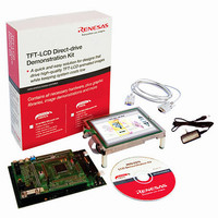
Manufacturer Part Number
YLCDRSK2378
Description
KIT DEV EVAL H8S/2378 LCD
Manufacturer
Renesas Electronics America
Series
H8®r
Datasheet
1.YR0K42378FC000BA.pdf
(1208 pages)
Specifications of YLCDRSK2378
Main Purpose
Displays, LCD Controller
Embedded
Yes, MCU, 16-Bit
Utilized Ic / Part
YLCDRSK2378
Primary Attributes
5.7" QVGA, Touch Screen
Secondary Attributes
Source Code on CD, Debugging Requires Emulator Cable E10A USB/JTAG
Lead Free Status / RoHS Status
Lead free / RoHS Compliant


9.7.2
An example of DTC chain transfer is shown in which pulse output is performed using the PPG.
Chain transfer can be used to perform pulse output data transfer and PPG output trigger cycle
updating. Repeat mode transfer to NDR of the PPG is performed in the first half of the chain
transfer, and normal mode transfer to the TPU’s TGR in the second half. This is because clearing
of the activation source and interrupt generation at the end of the specified number of transfers are
restricted to the second half of the chain transfer (transfer when CHNE = 0).
1. Perform settings for transfer to NDR of the PPG. Set MRA to source address incrementing
2. Perform settings for transfer to the TPU’s TGR. Set MRA to source address incrementing
3. Locate the TPU transfer register information consecutively after the NDR transfer register
4. Set the start address of the NDR transfer register information to the DTC vector address.
5. Set the bit corresponding to TGIA in DTCER to 1.
6. Set TGRA as an output compare register (output disabled) with TIOR, and enable the TGIA
7. Set the initial output value in PODR, and the next output value in NDR. Set bits in DDR and
8. Set the CST bit in TSTR to 1, and start the TCNT count operation.
9. Each time a TGRA compare match occurs, the next output value is transferred to NDR and the
10. When the specified number of transfers are completed (the TPU transfer CRA value is 0), the
(SM1 = 1, SM0 = 0), fixed destination address (DM1 = DM0 = 0), repeat mode (MD1 = 0,
MD0 = 1), and word size (Sz = 1). Set the source side as a repeat area (DTS = 1). Set MRB to
chain mode (CHNE = 1, DISEL = 0). Set the data table start address in SAR, the NDRH
address in DAR, and the data table size in CRAH and CRAL. CRB can be set to any value.
(SM1 = 1, SM0 = 0), fixed destination address (DM1 = DM0 = 0), normal mode (MD1 = MD0
= 0), and word size (Sz = 1). Set the data table start address in SAR, the TGRA address in
DAR, and the data table size in CRA. CRB can be set to any value.
information.
interrupt with TIER.
NDER for which output is to be performed to 1. Using PCR, select the TPU compare match to
be used as the output trigger.
set value of the next output trigger period is transferred to TGRA. The activation source TGFA
flag is cleared.
TGFA flag is held at 1, the DTCE bit is cleared to 0, and a TGIA interrupt request is sent to the
CPU. Termination processing should be performed in the interrupt handling routine.
Chain Transfer
Rev.7.00 Mar. 18, 2009 page 449 of 1136
Section 9 Data Transfer Controller (DTC)
REJ09B0109-0700
Related parts for YLCDRSK2378
Image
Part Number
Description
Manufacturer
Datasheet
Request
R

Part Number:
Description:
KIT STARTER FOR M16C/29
Manufacturer:
Renesas Electronics America
Datasheet:

Part Number:
Description:
KIT STARTER FOR R8C/2D
Manufacturer:
Renesas Electronics America
Datasheet:

Part Number:
Description:
R0K33062P STARTER KIT
Manufacturer:
Renesas Electronics America
Datasheet:

Part Number:
Description:
KIT STARTER FOR R8C/23 E8A
Manufacturer:
Renesas Electronics America
Datasheet:

Part Number:
Description:
KIT STARTER FOR R8C/25
Manufacturer:
Renesas Electronics America
Datasheet:

Part Number:
Description:
KIT STARTER H8S2456 SHARPE DSPLY
Manufacturer:
Renesas Electronics America
Datasheet:

Part Number:
Description:
KIT STARTER FOR R8C38C
Manufacturer:
Renesas Electronics America
Datasheet:

Part Number:
Description:
KIT STARTER FOR R8C35C
Manufacturer:
Renesas Electronics America
Datasheet:

Part Number:
Description:
KIT STARTER FOR R8CL3AC+LCD APPS
Manufacturer:
Renesas Electronics America
Datasheet:
Part Number:
Description:
KIT STARTER FOR RX610
Manufacturer:
Renesas Electronics America
Datasheet:

Part Number:
Description:
KIT STARTER FOR R32C/118
Manufacturer:
Renesas Electronics America
Datasheet:

Part Number:
Description:
KIT DEV RSK-R8C/26-29
Manufacturer:
Renesas Electronics America
Datasheet:

Part Number:
Description:
KIT STARTER FOR SH7124
Manufacturer:
Renesas Electronics America
Datasheet:

Part Number:
Description:
KIT STARTER FOR H8SX/1622
Manufacturer:
Renesas Electronics America
Datasheet:

Part Number:
Description:
KIT DEV FOR SH7203
Manufacturer:
Renesas Electronics America
Datasheet: