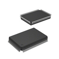
DF2367VF33 Renesas Electronics America, DF2367VF33 Datasheet - Page 715

DF2367VF33
Manufacturer Part Number
DF2367VF33
Description
MCU 3V 384K 128-QFP
Manufacturer
Renesas Electronics America
Series
H8® H8S/2300r
Datasheet
1.DF2368VTE34V.pdf
(1044 pages)
Specifications of DF2367VF33
Core Processor
H8S/2000
Core Size
16-Bit
Speed
33MHz
Connectivity
I²C, IrDA, SCI, SmartCard
Peripherals
DMA, POR, PWM, WDT
Number Of I /o
84
Program Memory Size
384KB (384K x 8)
Program Memory Type
FLASH
Ram Size
24K x 8
Voltage - Supply (vcc/vdd)
3 V ~ 3.6 V
Data Converters
A/D 10x10b, D/A 2x8b
Oscillator Type
Internal
Operating Temperature
-20°C ~ 75°C
Package / Case
128-QFP
Lead Free Status / RoHS Status
Contains lead / RoHS non-compliant
Eeprom Size
-
Other names
HD64F2367VF33
HD64F2367VF33
HD64F2367VF33
Available stocks
Company
Part Number
Manufacturer
Quantity
Price
Company:
Part Number:
DF2367VF33V
Manufacturer:
Renesas Electronics America
Quantity:
135
Company:
Part Number:
DF2367VF33V
Manufacturer:
Renesas Electronics America
Quantity:
10 000
Company:
Part Number:
DF2367VF33WV
Manufacturer:
Renesas Electronics America
Quantity:
10 000
- Current page: 715 of 1044
- Download datasheet (6Mb)
Note: * Prevent any interrupts while steps [1] to [3] are executed.
Additional information: When receiving one-byte data, execute step [1], and then step [7] omitting steps [2] to [6].
No
No
No
Set ACKBT = 0 (ICIER)
Set ACKBT = 1 (ICIER)
Set RCVD = 0 (ICCRA)
Set RCVD - 1 (ICCRA)
Clear ACKBT of ICIER
Set TRS = 0 (ICCRA)
Set MST = 0 (ICCRA)
Clear TDRE of ICSR
Dummy read ICDRR
Read RDRF in ICSR
Read RDRF in ICSR
Clear STOP of ICSR
Read STOP of ICSR
Clear TEND in ICSR
Mater receive mode
Write BBSY = 0
Read ICDRR
Read ICDRR
Read ICDRR
(Last receive
and SCP = 0
RDRF=1 ?
RDRF=1 ?
STOP=1 ?
Figure 15.15 Sample Flowchart for Master Receive Mode
- 1)?
End
Yes
Yes
Yes
No
In step [8], dummy read ICDRR.
Yes
[1]
[2]
[3]
[4]
[5]
[6]
[7]
[8]
[9]
[10]
[11]
[12]
[13]
[14]
[15]
[16]
[1]
[2]
[3]
[4]
[5]
[6]
[7]
[8]
[9]
[10] Clear STOP flag.
[11] Stop condition issuance
[12] Wait for the creation of stop condition.
[13] Read the receive data of the final byte, and clear RDRF to 0.
[14] Clear RCVD to 0.
[15] Clear ACKBT.
[16] Set slave receive mode.
Clear TEND, select master receive mode, and then clear TDRE. *
Set acknowledge to the transmitting device. *
Dummy read ICDDR *
Wait for 1 byte to be received.
Check if (last receive - 1)
Read the receive data, and clear RDRF to 0.
Set acknowledge of the final byte. Disable continuous receive (RCVD = 1).
Read receive data of (final byte - 1), and clear RDRF to 0.
Wait for the final byte to be received.
Section 15 I
Rev.6.00 Mar. 18, 2009 Page 655 of 980
2
C Bus Interface2 (IIC2) (Option)
REJ09B0050-0600
Related parts for DF2367VF33
Image
Part Number
Description
Manufacturer
Datasheet
Request
R

Part Number:
Description:
CONN PLUG 12POS DUAL 0.5MM SMD
Manufacturer:
Hirose Electric Co Ltd
Datasheet:

Part Number:
Description:
CONN PLUG 18POS DUAL 0.5MM SMD
Manufacturer:
Hirose Electric Co Ltd
Datasheet:

Part Number:
Description:
CONN PLUG 14POS DUAL 0.5MM SMD
Manufacturer:
Hirose Electric Co Ltd
Datasheet:

Part Number:
Description:
CONN RECEPT 20POS DUAL 0.5MM SMD
Manufacturer:
Hirose Electric Co Ltd
Datasheet:

Part Number:
Description:
CONN PLUG 16POS DUAL 0.5MM SMD
Manufacturer:
Hirose Electric Co Ltd
Datasheet:

Part Number:
Description:
CONN RECEPT 16POS DUAL 0.5MM SMD
Manufacturer:
Hirose Electric Co Ltd
Datasheet:

Part Number:
Description:
CONN PLUG 20POS DUAL 0.5MM SMD
Manufacturer:
Hirose Electric Co Ltd
Datasheet:

Part Number:
Description:
CONN PLUG 30POS DUAL 0.5MM SMD
Manufacturer:
Hirose Electric Co Ltd
Datasheet:

Part Number:
Description:
CONN RECEPT 30POS DUAL 0.5MM SMD
Manufacturer:
Hirose Electric Co Ltd
Datasheet:

Part Number:
Description:
CONN PLUG 40POS DUAL 0.5MM SMD
Manufacturer:
Hirose Electric Co Ltd
Datasheet:

Part Number:
Description:
KIT STARTER FOR M16C/29
Manufacturer:
Renesas Electronics America
Datasheet:

Part Number:
Description:
KIT STARTER FOR R8C/2D
Manufacturer:
Renesas Electronics America
Datasheet:

Part Number:
Description:
R0K33062P STARTER KIT
Manufacturer:
Renesas Electronics America
Datasheet:

Part Number:
Description:
KIT STARTER FOR R8C/23 E8A
Manufacturer:
Renesas Electronics America
Datasheet:

Part Number:
Description:
KIT STARTER FOR R8C/25
Manufacturer:
Renesas Electronics America
Datasheet:


