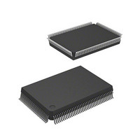
DF2367VF33 Renesas Electronics America, DF2367VF33 Datasheet - Page 393

DF2367VF33
Manufacturer Part Number
DF2367VF33
Description
MCU 3V 384K 128-QFP
Manufacturer
Renesas Electronics America
Series
H8® H8S/2300r
Datasheet
1.DF2368VTE34V.pdf
(1044 pages)
Specifications of DF2367VF33
Core Processor
H8S/2000
Core Size
16-Bit
Speed
33MHz
Connectivity
I²C, IrDA, SCI, SmartCard
Peripherals
DMA, POR, PWM, WDT
Number Of I /o
84
Program Memory Size
384KB (384K x 8)
Program Memory Type
FLASH
Ram Size
24K x 8
Voltage - Supply (vcc/vdd)
3 V ~ 3.6 V
Data Converters
A/D 10x10b, D/A 2x8b
Oscillator Type
Internal
Operating Temperature
-20°C ~ 75°C
Package / Case
128-QFP
Lead Free Status / RoHS Status
Contains lead / RoHS non-compliant
Eeprom Size
-
Other names
HD64F2367VF33
HD64F2367VF33
HD64F2367VF33
Available stocks
Company
Part Number
Manufacturer
Quantity
Price
Company:
Part Number:
DF2367VF33V
Manufacturer:
Renesas Electronics America
Quantity:
135
Company:
Part Number:
DF2367VF33V
Manufacturer:
Renesas Electronics America
Quantity:
10 000
Company:
Part Number:
DF2367VF33WV
Manufacturer:
Renesas Electronics America
Quantity:
10 000
- Current page: 393 of 1044
- Download datasheet (6Mb)
• P13/PO11/TIOCD0/TCLKB/TEND1
Notes: 1. TIOCD0 input when MD3 to MD0 = B'0000 and IOD3 to IOD0 = B'10××.
Legend:
×: Don’t care
TEE1
TPU channel 0
settings
P13DDR
NDER11
Pin function
TPU channel 0
settings
MD3 to MD0
IOD3 to IOD0
CCLR2, CCLR0
Output function
The pin function is switched as shown below according to the combination of the TPU channel
0 settings (by bits MD3 to MD0 in TMDR_0, bits IOD3 to IOD0 in TIOR0L, and bits CCLR2
to CCLR0 in TCR_0), bits TPSC2 to TPSC0 in TCR_0 to TCR_2, bit NDER11 in NDERH,
bit TEE1 in DMATCR of DMAC and bit P13DDR.
2. TCLKB input when the setting for any of TCR_0 to TCR_2 is TPSC2 to TPSC0 = B'101.
TCLKB input when phase counting mode is set for channels 1 and 5.
(1) in table below
TIOCD0 output
B'0000
B'0100
B'1×××
(2)
—
—
—
—
B'0000
B'0001 to
B'0101 to
compare
B'0011
B'0111
Output
output
(1)
—
P13 input
TCLKB input *
—
(2) in table below
0
B'0010
0
(2)
—
—
—
TIOCD0 input *
P13 output
2
Rev.6.00 Mar. 18, 2009 Page 333 of 980
1
0
B'××00
(2)
—
—
1
PO11 output
PWM mode
—
Other than
1
1
2 output
B'0011
B'110
Other than B'××00
(1)
Section 9 I/O Ports
REJ09B0050-0600
TEND1 output
—
—
—
B'110
1
(2)
—
Related parts for DF2367VF33
Image
Part Number
Description
Manufacturer
Datasheet
Request
R

Part Number:
Description:
CONN PLUG 12POS DUAL 0.5MM SMD
Manufacturer:
Hirose Electric Co Ltd
Datasheet:

Part Number:
Description:
CONN PLUG 18POS DUAL 0.5MM SMD
Manufacturer:
Hirose Electric Co Ltd
Datasheet:

Part Number:
Description:
CONN PLUG 14POS DUAL 0.5MM SMD
Manufacturer:
Hirose Electric Co Ltd
Datasheet:

Part Number:
Description:
CONN RECEPT 20POS DUAL 0.5MM SMD
Manufacturer:
Hirose Electric Co Ltd
Datasheet:

Part Number:
Description:
CONN PLUG 16POS DUAL 0.5MM SMD
Manufacturer:
Hirose Electric Co Ltd
Datasheet:

Part Number:
Description:
CONN RECEPT 16POS DUAL 0.5MM SMD
Manufacturer:
Hirose Electric Co Ltd
Datasheet:

Part Number:
Description:
CONN PLUG 20POS DUAL 0.5MM SMD
Manufacturer:
Hirose Electric Co Ltd
Datasheet:

Part Number:
Description:
CONN PLUG 30POS DUAL 0.5MM SMD
Manufacturer:
Hirose Electric Co Ltd
Datasheet:

Part Number:
Description:
CONN RECEPT 30POS DUAL 0.5MM SMD
Manufacturer:
Hirose Electric Co Ltd
Datasheet:

Part Number:
Description:
CONN PLUG 40POS DUAL 0.5MM SMD
Manufacturer:
Hirose Electric Co Ltd
Datasheet:

Part Number:
Description:
KIT STARTER FOR M16C/29
Manufacturer:
Renesas Electronics America
Datasheet:

Part Number:
Description:
KIT STARTER FOR R8C/2D
Manufacturer:
Renesas Electronics America
Datasheet:

Part Number:
Description:
R0K33062P STARTER KIT
Manufacturer:
Renesas Electronics America
Datasheet:

Part Number:
Description:
KIT STARTER FOR R8C/23 E8A
Manufacturer:
Renesas Electronics America
Datasheet:

Part Number:
Description:
KIT STARTER FOR R8C/25
Manufacturer:
Renesas Electronics America
Datasheet:


