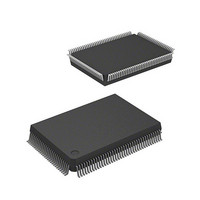
DF2367VF33 Renesas Electronics America, DF2367VF33 Datasheet - Page 706

DF2367VF33
Manufacturer Part Number
DF2367VF33
Description
MCU 3V 384K 128-QFP
Manufacturer
Renesas Electronics America
Series
H8® H8S/2300r
Datasheet
1.DF2368VTE34V.pdf
(1044 pages)
Specifications of DF2367VF33
Core Processor
H8S/2000
Core Size
16-Bit
Speed
33MHz
Connectivity
I²C, IrDA, SCI, SmartCard
Peripherals
DMA, POR, PWM, WDT
Number Of I /o
84
Program Memory Size
384KB (384K x 8)
Program Memory Type
FLASH
Ram Size
24K x 8
Voltage - Supply (vcc/vdd)
3 V ~ 3.6 V
Data Converters
A/D 10x10b, D/A 2x8b
Oscillator Type
Internal
Operating Temperature
-20°C ~ 75°C
Package / Case
128-QFP
Lead Free Status / RoHS Status
Contains lead / RoHS non-compliant
Eeprom Size
-
Other names
HD64F2367VF33
HD64F2367VF33
HD64F2367VF33
Available stocks
Company
Part Number
Manufacturer
Quantity
Price
Company:
Part Number:
DF2367VF33V
Manufacturer:
Renesas Electronics America
Quantity:
135
Company:
Part Number:
DF2367VF33V
Manufacturer:
Renesas Electronics America
Quantity:
10 000
Company:
Part Number:
DF2367VF33WV
Manufacturer:
Renesas Electronics America
Quantity:
10 000
- Current page: 706 of 1044
- Download datasheet (6Mb)
Section 15 I
15.4.3
In master receive mode, the master device outputs the receive clock, receives data from the slave
device, and returns an acknowledge signal. For master receive mode operation timing, refer to
figures 15.7 and 15.8. The reception procedure and operations in master receive mode are shown
below.
1. Clear the TEND bit in ICSR to 0, then clear the TRS bit in ICCRA to 0 to switch from master
2. When ICDRR is read (dummy data read), reception is started, and the receive clock is output,
3. After the reception of first frame data is completed, the RDRF bit in ICST is set to 1 at the rise
4. The continuous reception is performed by reading ICDRR and clearing RDRF to 0 every time
5. If next frame is the last receive data, set the RCVD bit in ICCR1 to 1 before reading ICDRR.
6. When the RDRF bit is set to 1 at rise of the 9th receive clock pulse, read ICDRR. Then, clear
Rev.6.00 Mar. 18, 2009 Page 646 of 980
REJ09B0050-0600
(master output)
(master output)
(slave output)
transmit mode to master receive mode. Then, clear the TDRE bit to 0.
and data received, in synchronization with the internal clock. The master device outputs the
level specified by ACKBT in ICIER to SDA, at the 9th receive clock pulse.
of 9th receive clock pulse. At this time, the received data is read by reading ICDRR.
RDRF is set. If 8th receive clock pulse falls after reading ICDRR by the other processing while
RDRF is 1, SCL is fixed low until ICDRR is read.
This enables the issuance of the stop condition after the next reception.
RCVD.
processing
SCL
ICDRS
SDA
SDA
ICDRT
TDRE
TEND
User
Master Receive Operation
2
C Bus Interface2 (IIC2) (Option)
[5] Write data to ICDRT. Clear TDRE.
Figure 15.6 Master Transmit Mode Operation Timing 2
A
9
Bit 7
1
Bit 6
2
Bit 5
3
Data n
Data n
Bit 4
4
Bit 3
5
Bit 2
6
[6] Issue stop condition. Clear TEND.
Bit 1
7
Bit 0
8
[7] Set slave receive mode
A/
9
Related parts for DF2367VF33
Image
Part Number
Description
Manufacturer
Datasheet
Request
R

Part Number:
Description:
CONN PLUG 12POS DUAL 0.5MM SMD
Manufacturer:
Hirose Electric Co Ltd
Datasheet:

Part Number:
Description:
CONN PLUG 18POS DUAL 0.5MM SMD
Manufacturer:
Hirose Electric Co Ltd
Datasheet:

Part Number:
Description:
CONN PLUG 14POS DUAL 0.5MM SMD
Manufacturer:
Hirose Electric Co Ltd
Datasheet:

Part Number:
Description:
CONN RECEPT 20POS DUAL 0.5MM SMD
Manufacturer:
Hirose Electric Co Ltd
Datasheet:

Part Number:
Description:
CONN PLUG 16POS DUAL 0.5MM SMD
Manufacturer:
Hirose Electric Co Ltd
Datasheet:

Part Number:
Description:
CONN RECEPT 16POS DUAL 0.5MM SMD
Manufacturer:
Hirose Electric Co Ltd
Datasheet:

Part Number:
Description:
CONN PLUG 20POS DUAL 0.5MM SMD
Manufacturer:
Hirose Electric Co Ltd
Datasheet:

Part Number:
Description:
CONN PLUG 30POS DUAL 0.5MM SMD
Manufacturer:
Hirose Electric Co Ltd
Datasheet:

Part Number:
Description:
CONN RECEPT 30POS DUAL 0.5MM SMD
Manufacturer:
Hirose Electric Co Ltd
Datasheet:

Part Number:
Description:
CONN PLUG 40POS DUAL 0.5MM SMD
Manufacturer:
Hirose Electric Co Ltd
Datasheet:

Part Number:
Description:
KIT STARTER FOR M16C/29
Manufacturer:
Renesas Electronics America
Datasheet:

Part Number:
Description:
KIT STARTER FOR R8C/2D
Manufacturer:
Renesas Electronics America
Datasheet:

Part Number:
Description:
R0K33062P STARTER KIT
Manufacturer:
Renesas Electronics America
Datasheet:

Part Number:
Description:
KIT STARTER FOR R8C/23 E8A
Manufacturer:
Renesas Electronics America
Datasheet:

Part Number:
Description:
KIT STARTER FOR R8C/25
Manufacturer:
Renesas Electronics America
Datasheet:


