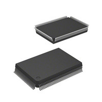
DF2367VF33 Renesas Electronics America, DF2367VF33 Datasheet - Page 210

DF2367VF33
Manufacturer Part Number
DF2367VF33
Description
MCU 3V 384K 128-QFP
Manufacturer
Renesas Electronics America
Series
H8® H8S/2300r
Datasheet
1.DF2368VTE34V.pdf
(1044 pages)
Specifications of DF2367VF33
Core Processor
H8S/2000
Core Size
16-Bit
Speed
33MHz
Connectivity
I²C, IrDA, SCI, SmartCard
Peripherals
DMA, POR, PWM, WDT
Number Of I /o
84
Program Memory Size
384KB (384K x 8)
Program Memory Type
FLASH
Ram Size
24K x 8
Voltage - Supply (vcc/vdd)
3 V ~ 3.6 V
Data Converters
A/D 10x10b, D/A 2x8b
Oscillator Type
Internal
Operating Temperature
-20°C ~ 75°C
Package / Case
128-QFP
Lead Free Status / RoHS Status
Contains lead / RoHS non-compliant
Eeprom Size
-
Other names
HD64F2367VF33
HD64F2367VF33
HD64F2367VF33
Available stocks
Company
Part Number
Manufacturer
Quantity
Price
Company:
Part Number:
DF2367VF33V
Manufacturer:
Renesas Electronics America
Quantity:
135
Company:
Part Number:
DF2367VF33V
Manufacturer:
Renesas Electronics America
Quantity:
10 000
Company:
Part Number:
DF2367VF33WV
Manufacturer:
Renesas Electronics America
Quantity:
10 000
- Current page: 210 of 1044
- Download datasheet (6Mb)
Section 6 Bus Controller (BSC)
6.5
The basic bus interface enables direct connection of ROM, SRAM, and so on.
6.5.1
Data sizes for the CPU and other internal bus masters are byte, word, and longword. The bus
controller has a data alignment function, and when accessing external space, controls whether the
upper data bus (D15 to D8) or lower data bus (D7 to D0) is used according to the bus
specifications for the area being accessed (8-bit access space or 16-bit access space) and the data
size.
8-Bit Access Space: Figure 6.7 illustrates data alignment control for the 8-bit access space. With
the 8-bit access space, the upper data bus (D15 to D8) is always used for accesses. The amount of
data that can be accessed at one time is one byte: a word access is performed as two byte accesses,
and a longword access, as four byte accesses.
Rev.6.00 Mar. 18, 2009 Page 150 of 980
REJ09B0050-0600
Basic Bus Interface
Data Size and Data Alignment
Address bus
Figure 6.6 CSn Signal Output Timing (n = 0 to 7)
T
1
Area n external address
Bus cycle
T
2
T
3
Related parts for DF2367VF33
Image
Part Number
Description
Manufacturer
Datasheet
Request
R

Part Number:
Description:
CONN PLUG 12POS DUAL 0.5MM SMD
Manufacturer:
Hirose Electric Co Ltd
Datasheet:

Part Number:
Description:
CONN PLUG 18POS DUAL 0.5MM SMD
Manufacturer:
Hirose Electric Co Ltd
Datasheet:

Part Number:
Description:
CONN PLUG 14POS DUAL 0.5MM SMD
Manufacturer:
Hirose Electric Co Ltd
Datasheet:

Part Number:
Description:
CONN RECEPT 20POS DUAL 0.5MM SMD
Manufacturer:
Hirose Electric Co Ltd
Datasheet:

Part Number:
Description:
CONN PLUG 16POS DUAL 0.5MM SMD
Manufacturer:
Hirose Electric Co Ltd
Datasheet:

Part Number:
Description:
CONN RECEPT 16POS DUAL 0.5MM SMD
Manufacturer:
Hirose Electric Co Ltd
Datasheet:

Part Number:
Description:
CONN PLUG 20POS DUAL 0.5MM SMD
Manufacturer:
Hirose Electric Co Ltd
Datasheet:

Part Number:
Description:
CONN PLUG 30POS DUAL 0.5MM SMD
Manufacturer:
Hirose Electric Co Ltd
Datasheet:

Part Number:
Description:
CONN RECEPT 30POS DUAL 0.5MM SMD
Manufacturer:
Hirose Electric Co Ltd
Datasheet:

Part Number:
Description:
CONN PLUG 40POS DUAL 0.5MM SMD
Manufacturer:
Hirose Electric Co Ltd
Datasheet:

Part Number:
Description:
KIT STARTER FOR M16C/29
Manufacturer:
Renesas Electronics America
Datasheet:

Part Number:
Description:
KIT STARTER FOR R8C/2D
Manufacturer:
Renesas Electronics America
Datasheet:

Part Number:
Description:
R0K33062P STARTER KIT
Manufacturer:
Renesas Electronics America
Datasheet:

Part Number:
Description:
KIT STARTER FOR R8C/23 E8A
Manufacturer:
Renesas Electronics America
Datasheet:

Part Number:
Description:
KIT STARTER FOR R8C/25
Manufacturer:
Renesas Electronics America
Datasheet:


