8.10.00 J-TRACE ARM Segger Microcontroller Systems, 8.10.00 J-TRACE ARM Datasheet - Page 172
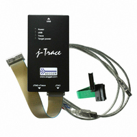
8.10.00 J-TRACE ARM
Manufacturer Part Number
8.10.00 J-TRACE ARM
Description
JTAG EMULATOR ARM7/ARM9 ETM
Manufacturer
Segger Microcontroller Systems
Type
Emulatorr
Specifications of 8.10.00 J-TRACE ARM
Contents
Emulation Module
For Use With/related Products
ARM7, ARM9
Lead Free Status / RoHS Status
Lead free / RoHS Compliant
Other names
899-1006


172
8.1
8.1.1
J-Link / J-Trace (UM08001)
J-Link and J-Trace have a JTAG connector compati-
ble to ARM’s Multi-ICE. The JTAG connector is a 20
way Insulation Displacement Connector (IDC) keyed
box header (2.54mm male) that mates with IDC
sockets mounted on a ribbon cable.
The following table lists the J-Link / J-Trace JTAG
pinout.
Table 8.1: J-Link / J-Trace pinout
11
13
15
17
19
PIN
1
2
3
5
7
9
20-pin JTAG/SWD connector
Pinout for JTAG
VTref
Not con-
nected
nTRST
TDI
TMS
TCK
RTCK
TDO
RESET
DBGRQ
5V-Sup-
ply
SIGNAL
Input
NC
Output
Output
Output
Output
Input
Input
I/O
NC
Output
TYPE
This is the target reference voltage. It is used to check if
the target has power, to create the logic-level reference for
the input comparators and to control the output logic levels
to the target. It is normally fed from Vdd of the target board
and must not have a series resistor.
This pin is not connected in J-Link.
JTAG Reset. Output from J-Link to the Reset signal of the
target JTAG port. Typically connected to nTRST of the target
CPU. This pin is normally pulled HIGH on the target to avoid
unintentional resets when there is no connection.
JTAG data input of target CPU.- It is recommended that this
pin is pulled to a defined state on the target board. Typically
connected to TDI of the target CPU.
JTAG mode set input of target CPU. This pin should be
pulled up on the target. Typically connected to TMS of the
target CPU.
JTAG clock signal to target CPU. It is recommended that this
pin is pulled to a defined state of the target board. Typically
connected to TCK of the target CPU.
Return test clock signal from the target. Some targets must
synchronize the JTAG inputs to internal clocks. To assist in
meeting this requirement, you can use a returned, and
retimed, TCK to dynamically control the TCK rate. J-Link
supports adaptive clocking, which waits for TCK changes to
be echoed correctly before making further changes. Con-
nect to RTCK if available, otherwise to GND.
JTAG data output from target CPU. Typically connected to
TDO of the target CPU.
Target CPU reset signal. Typically connected to the RESET
pin of the target CPU, which is typically called "nRST",
"nRESET" or "RESET".
This pin is not connected in J-Link. It is reserved for com-
patibility with other equipment to be used as a debug
request signal to the target system. Typically connected to
DBGRQ if available, otherwise left open.
This pin can be used to supply power to the target hard-
ware. Older J-Links may not be able to supply power on this
pin. For more information about how to enable/disable the
power supply, please refer to Target power supply on
page 174.
CHAPTER 8
© 2004-2011 SEGGER Microcontroller GmbH & Co. KG
Description
VTref
nTRST
TDI
TMS
TCK
RTCK
TDO
RESET
DBGRQ
5V-Supply
Target interfaces and adapters
11
13
15
17
19
1
3
5
7
9
12
2
4
6
8
10
14
16
18
20
NC
GND
GND
GND
GND
GND
GND
GND
GND
GND
Related parts for 8.10.00 J-TRACE ARM
Image
Part Number
Description
Manufacturer
Datasheet
Request
R

Part Number:
Description:
CONNECTOR JTAG-ARM ISOLATION
Manufacturer:
Segger Microcontroller Systems
Datasheet:

Part Number:
Description:
ADAPTER ARM TARGET 14PIN RIBBON
Manufacturer:
Segger Microcontroller Systems
Datasheet:

Part Number:
Description:
JTAG EMULATOR FOR ARM CORES
Manufacturer:
Segger Microcontroller Systems
Datasheet:

Part Number:
Description:
JTAG EMULATOR FOR ARM CORES
Manufacturer:
Segger Microcontroller Systems
Datasheet:

Part Number:
Description:
PROGRAMMING TOOL FOR MCU
Manufacturer:
Segger Microcontroller Systems
Datasheet:

Part Number:
Description:
PROGRAMMING TOOL FOR ST7 MCU
Manufacturer:
Segger Microcontroller Systems
Datasheet:

Part Number:
Description:
PROGRAMMING TOOL FOR STM8
Manufacturer:
Segger Microcontroller Systems
Datasheet:

Part Number:
Description:
PROGRAMMER JTAG FOR ARM CORES
Manufacturer:
Segger Microcontroller Systems
Datasheet:

Part Number:
Description:
JTAG EMULATOR USB ETHERNET ARM
Manufacturer:
Segger Microcontroller Systems
Datasheet:

Part Number:
Description:
EMULATOR JTAG/SWD CORTEX M3
Manufacturer:
Segger Microcontroller Systems
Datasheet: