8.10.00 J-TRACE ARM Segger Microcontroller Systems, 8.10.00 J-TRACE ARM Datasheet - Page 151
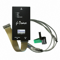
8.10.00 J-TRACE ARM
Manufacturer Part Number
8.10.00 J-TRACE ARM
Description
JTAG EMULATOR ARM7/ARM9 ETM
Manufacturer
Segger Microcontroller Systems
Type
Emulatorr
Specifications of 8.10.00 J-TRACE ARM
Contents
Emulation Module
For Use With/related Products
ARM7, ARM9
Lead Free Status / RoHS Status
Lead free / RoHS Compliant
Other names
899-1006


6.5.2
6.5.3
6.5.4
J-Link / J-Trace (UM08001)
Save the settings file and restart the debug session. Open the J-Link Control Panel
and verify that the "MemMap" tab shows the new settings for CFI flash and work RAM
area.
The configuration for the J-Link GDB Server is done by the .gdbinit file. The follow-
ing commands has to be added to the .gdbinit file to enable J-Link ARM FlashDL and
FlashBPs:
monitor WorkRAM = <SAddr>-<EAddr>
monitor flash CFI = <SAddr>-<EAddr>
monitor flash download = 1
monitor flash breakpoints = 1
For more information about these four commands please refer to UM08005, J-Link
GDB Server User Guide chapter Supported remote commands.
The following command sequence shows how to perform a download into external,
CFI-compliant, parallel NOR-Flash on a ST STM32F103ZE using J-Link commander:
r
speed 1000
exec setcfiflash 0x64000000 - 0x64FFFFFF
exec setworkram 0x20000000 - 0x2000FFFF
w4 0x40021014, 0x00000114 // RCC_AHBENR, FSMC clock enable
w4 0x40021018, 0x000001FD // GPIOD~G clock enable
w4 0x40011400, 0xB4BB44BB // GPIOD low config, NOE, NWE => Output, NWAIT => Input
w4 0x40011404, 0xBBBBBBBB // GPIOD high config, A16-A18
w4 0x40011800, 0xBBBBBBBB // GPIOE low config, A19-A23
w4 0x40011804, 0xBBBBBBBB // GPIOE high config, D5-D12
w4 0x40011C00, 0x44BBBBBB // GPIOF low config, A0-A5
w4 0x40011C04, 0xBBBB4444 // GPIOF high config, A6-A9
w4 0x40012000, 0x44BBBBBB // GPIOG low config, A10-A15
w4 0x40012004, 0x444B4BB4 // GPIOG high config, NE2 => output
w4 0xA0000008, 0x00001059 // CS control reg 2, 16-bit, write enable, Type: NOR flash
w4 0xA000000C, 0x10000505 // CS2 timing reg (read access)
w4 0xA000010C, 0x10000505 // CS2 timing reg (write access)
speed 4000
mem 0x64000000,100
loadbin C:\STMB672_STM32F103ZE_TestBlinky.bin,0x64000000
mem 0x64000000,100
Currently J-Link RDI supports internal flash memory only.
J-Link GDB Server
J-Link commander
J-Link RDI
© 2004-2011 SEGGER Microcontroller GmbH & Co. KG
151
Related parts for 8.10.00 J-TRACE ARM
Image
Part Number
Description
Manufacturer
Datasheet
Request
R

Part Number:
Description:
CONNECTOR JTAG-ARM ISOLATION
Manufacturer:
Segger Microcontroller Systems
Datasheet:

Part Number:
Description:
ADAPTER ARM TARGET 14PIN RIBBON
Manufacturer:
Segger Microcontroller Systems
Datasheet:

Part Number:
Description:
JTAG EMULATOR FOR ARM CORES
Manufacturer:
Segger Microcontroller Systems
Datasheet:

Part Number:
Description:
JTAG EMULATOR FOR ARM CORES
Manufacturer:
Segger Microcontroller Systems
Datasheet:

Part Number:
Description:
PROGRAMMING TOOL FOR MCU
Manufacturer:
Segger Microcontroller Systems
Datasheet:

Part Number:
Description:
PROGRAMMING TOOL FOR ST7 MCU
Manufacturer:
Segger Microcontroller Systems
Datasheet:

Part Number:
Description:
PROGRAMMING TOOL FOR STM8
Manufacturer:
Segger Microcontroller Systems
Datasheet:

Part Number:
Description:
PROGRAMMER JTAG FOR ARM CORES
Manufacturer:
Segger Microcontroller Systems
Datasheet:

Part Number:
Description:
JTAG EMULATOR USB ETHERNET ARM
Manufacturer:
Segger Microcontroller Systems
Datasheet:

Part Number:
Description:
EMULATOR JTAG/SWD CORTEX M3
Manufacturer:
Segger Microcontroller Systems
Datasheet: