R5F21162SP#U0 Renesas Electronics America, R5F21162SP#U0 Datasheet - Page 84
R5F21162SP#U0
Manufacturer Part Number
R5F21162SP#U0
Description
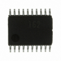
IC R8C MCU FLASH 8K 20SSOP
Manufacturer
Renesas Electronics America
Series
M16C™ M16C/R8C/Tiny/16r
Datasheets
1.R5F211A2SPU0.pdf
(300 pages)
2.R5F21173DSPU0.pdf
(40 pages)
3.R5F21173DSPU0.pdf
(281 pages)
Specifications of R5F21162SP#U0
Core Processor
R8C
Core Size
16-Bit
Speed
20MHz
Connectivity
I²C, SIO, UART/USART
Peripherals
LED, POR, Voltage Detect, WDT
Number Of I /o
13
Program Memory Size
8KB (8K x 8)
Program Memory Type
FLASH
Ram Size
512 x 8
Voltage - Supply (vcc/vdd)
2.7 V ~ 5.5 V
Data Converters
A/D 4x10b
Oscillator Type
Internal
Operating Temperature
-20°C ~ 85°C
Package / Case
20-SSOP
For Use With
R0K521134S000BE - KIT EVAL STARTER FOR R8C/13
Lead Free Status / RoHS Status
Lead free / RoHS Compliant
Eeprom Size
-


R8C/16 Group, R8C/17 Group
Rev.2.10
REJ09B0169-0210
11.2
Figure 11.11
11.2.1
External Input Enable Register
_______
INT0
b7 b6 b5
NOTES :
b7 b6 b5 b4 b3 b2 b1 b0
0
1.
2.
3.
0 0 0
The INT0 interrupt is generated by an INT0 input. When using the INT0 interrupt, the INT0EN bit in
the INTEN register is set to “1” (enable). The edge polarity is selected using the INT0PL bit in the
INTEN register and the POL bit in the INT0IC register.
Inputs can be passed through a digital filter with three different sampling clocks.
The INT0 pin is shared with the external trigger input pin of timer Z.
Figure 11.11 shows the INTEN and INT0F Registers.
Input Filter Select Register
INT Interrupt
Set the INT0EN bit w hile the INOSTG bit in the PUM register is set to “0” (one-shot trigger disabled).
When setting the INT0PL bit to “1” (both edges), set the POL bit in the INT0IC register to “0” (selects falling
edge).
The IR bit in the INT0IC register may be set to “1” (requests interrupt) w hen the INT0PL bit is rew ritten. Refer to 20.2.5
Changing Interrupt Factor.
Jan 19, 2006
b4
INT0 Interrupt
b3 b2 b1 b0
0 0
0
INTEN and INT0F Registers
Bit Symbol
Bit Symbol
(b7-b2)
(b7-b3)
Symbol
INT0EN
Symbol
INT0PL
INT0F0
INT0F1
INTEN
INT0F
(b2)
Page 69 of 254
—
—
—
_____
INT0
_____
INT0
Reserved Bit
_____
INT0
Reserved Bit
Nothing is assigned. When w rite, set to “0”.
When read, its content is indeterminate.
Input Enable Bit
Input Polarity Select Bit
Input Filter Select Bit
Address
Bit Name
001Eh
Address
Bit Name
0096h
(1)
(2,3)
b1 b0
0 0 : No filter
0 1 : Filter w ith f1 sampling
1 0 : Filter w ith f8 sampling
1 1 : Filter w ith f32 sampling
Set to “0”
0 : Disable
1 : Enable
0 : One edge
1 : Both edges
Set to “0”
After Reset
Function
After Reset
00h
Function
00h
11. Interrupt
RW
RW
RW
RW
RW
RW
RW
RW
—
Related parts for R5F21162SP#U0
Image
Part Number
Description
Manufacturer
Datasheet
Request
R

Part Number:
Description:
KIT STARTER FOR M16C/29
Manufacturer:
Renesas Electronics America
Datasheet:

Part Number:
Description:
KIT STARTER FOR R8C/2D
Manufacturer:
Renesas Electronics America
Datasheet:

Part Number:
Description:
R0K33062P STARTER KIT
Manufacturer:
Renesas Electronics America
Datasheet:

Part Number:
Description:
KIT STARTER FOR R8C/23 E8A
Manufacturer:
Renesas Electronics America
Datasheet:

Part Number:
Description:
KIT STARTER FOR R8C/25
Manufacturer:
Renesas Electronics America
Datasheet:

Part Number:
Description:
KIT STARTER H8S2456 SHARPE DSPLY
Manufacturer:
Renesas Electronics America
Datasheet:

Part Number:
Description:
KIT STARTER FOR R8C38C
Manufacturer:
Renesas Electronics America
Datasheet:

Part Number:
Description:
KIT STARTER FOR R8C35C
Manufacturer:
Renesas Electronics America
Datasheet:

Part Number:
Description:
KIT STARTER FOR R8CL3AC+LCD APPS
Manufacturer:
Renesas Electronics America
Datasheet:
Part Number:
Description:
KIT STARTER FOR RX610
Manufacturer:
Renesas Electronics America
Datasheet:

Part Number:
Description:
KIT STARTER FOR R32C/118
Manufacturer:
Renesas Electronics America
Datasheet:

Part Number:
Description:
KIT DEV RSK-R8C/26-29
Manufacturer:
Renesas Electronics America
Datasheet:

Part Number:
Description:
KIT STARTER FOR SH7124
Manufacturer:
Renesas Electronics America
Datasheet:

Part Number:
Description:
KIT STARTER FOR H8SX/1622
Manufacturer:
Renesas Electronics America
Datasheet:

Part Number:
Description:
KIT DEV FOR SH7203
Manufacturer:
Renesas Electronics America
Datasheet: