R5F21162SP#U0 Renesas Electronics America, R5F21162SP#U0 Datasheet - Page 159
R5F21162SP#U0
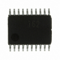
Manufacturer Part Number
R5F21162SP#U0
Description
IC R8C MCU FLASH 8K 20SSOP
Manufacturer
Renesas Electronics America
Series
M16C™ M16C/R8C/Tiny/16r
Datasheets
1.R5F211A2SPU0.pdf
(300 pages)
2.R5F21173DSPU0.pdf
(40 pages)
3.R5F21173DSPU0.pdf
(281 pages)
Specifications of R5F21162SP#U0
Core Processor
R8C
Core Size
16-Bit
Speed
20MHz
Connectivity
I²C, SIO, UART/USART
Peripherals
LED, POR, Voltage Detect, WDT
Number Of I /o
13
Program Memory Size
8KB (8K x 8)
Program Memory Type
FLASH
Ram Size
512 x 8
Voltage - Supply (vcc/vdd)
2.7 V ~ 5.5 V
Data Converters
A/D 4x10b
Oscillator Type
Internal
Operating Temperature
-20°C ~ 85°C
Package / Case
20-SSOP
For Use With
R0K521134S000BE - KIT EVAL STARTER FOR R8C/13
Lead Free Status / RoHS Status
Lead free / RoHS Compliant
Eeprom Size
-


R8C/16 Group, R8C/17 Group
Rev.2.10
REJ09B0169-0210
Figure 15.4
IIC Bus Control Register 2
b7 b6 b5 b4 b3 b2 b1
NOTES :
1.
2.
3.
4.
5. Refer to 20.6.1 Access of Registers Associated w ith IIC for the access of registers associated w ith IIC.
When w riting to the SDAO bit, w rite “0” to the SDAOP bit using the MOV instruction simultaneously.
Do not w rite during transfer operation.
This bit is enabled in master mode. When w rite to the BBSY bit, w rite “0” to the SCP bit using the MOV
instruction simultaneously. Execute the same w ay w hen the start condition is regenerating.
This bit is disabled w hen the clock synchronous serial format is used.
Jan 19, 2006
ICCR2 Register
b0
Bit Symbol
SDAOP
Symbol
IICRST
SDAO
ICCR2
SCLO
BBSY
(b0)
(b2)
SCP
Page 144 of 254
—
—
(5)
Nothing is assigned. When w rite, set to “0”.
When read, its content is “1”.
IIC Control Part Reset Bit When hang-up occurs due to communication failure
Nothing is assigned. When w rite, set to “0”.
When read, its content is “1”.
SCL Monitor Flag
SDAO Write Protect Bit
SDA Output Value
Control Bit
Start / Stop Condition
Generation Disable Bit
Bus Busy Bit
Address
Bit Name
00B9h
(4)
during I
control part of I
and initializing register.
0 : SCL pin is set to “L”
1 : SCL pin is set to “H”
When rew rite to SDAO bit, w rite “0” simultaneously
When read, its content is “1”.
When read
0 : SDA pin output is held “L”
1 : SDA pin output is held “H”
When w rite
0 : SDA pin output is changed to “L”
1 : SDA pin output is changed to high-impedance
When w rite to BBSY bit, w rite “0” simultaneously
When read, its content is “1”.
Writing “1” is disabled.
When read
0 : Bus is in released state
1 : Bus is in occupied state
When w rite
0 : Generates stop condition
1 : Generates start condition
(SDA signal changes from “H” to “L” w hile SCL
(“H” output is external pull-up resistor)
(SDA signal changes from “L” to “H” w hile SCL
signal is in “H” state)
signal is in “H” state)
2
C bus interface operation and w rite “1”, reset
(1,2)
(3)
2
C bus interface w ithout setting port
After Reset
01111101b
Function
15. I
2
C bus interface (IIC)
(3)
.
(1)
.
RW
RW
RW
RW
RW
RW
RO
—
—
Related parts for R5F21162SP#U0
Image
Part Number
Description
Manufacturer
Datasheet
Request
R

Part Number:
Description:
KIT STARTER FOR M16C/29
Manufacturer:
Renesas Electronics America
Datasheet:

Part Number:
Description:
KIT STARTER FOR R8C/2D
Manufacturer:
Renesas Electronics America
Datasheet:

Part Number:
Description:
R0K33062P STARTER KIT
Manufacturer:
Renesas Electronics America
Datasheet:

Part Number:
Description:
KIT STARTER FOR R8C/23 E8A
Manufacturer:
Renesas Electronics America
Datasheet:

Part Number:
Description:
KIT STARTER FOR R8C/25
Manufacturer:
Renesas Electronics America
Datasheet:

Part Number:
Description:
KIT STARTER H8S2456 SHARPE DSPLY
Manufacturer:
Renesas Electronics America
Datasheet:

Part Number:
Description:
KIT STARTER FOR R8C38C
Manufacturer:
Renesas Electronics America
Datasheet:

Part Number:
Description:
KIT STARTER FOR R8C35C
Manufacturer:
Renesas Electronics America
Datasheet:

Part Number:
Description:
KIT STARTER FOR R8CL3AC+LCD APPS
Manufacturer:
Renesas Electronics America
Datasheet:
Part Number:
Description:
KIT STARTER FOR RX610
Manufacturer:
Renesas Electronics America
Datasheet:

Part Number:
Description:
KIT STARTER FOR R32C/118
Manufacturer:
Renesas Electronics America
Datasheet:

Part Number:
Description:
KIT DEV RSK-R8C/26-29
Manufacturer:
Renesas Electronics America
Datasheet:

Part Number:
Description:
KIT STARTER FOR SH7124
Manufacturer:
Renesas Electronics America
Datasheet:

Part Number:
Description:
KIT STARTER FOR H8SX/1622
Manufacturer:
Renesas Electronics America
Datasheet:

Part Number:
Description:
KIT DEV FOR SH7203
Manufacturer:
Renesas Electronics America
Datasheet: