R5F21162SP#U0 Renesas Electronics America, R5F21162SP#U0 Datasheet - Page 23
R5F21162SP#U0
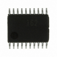
Manufacturer Part Number
R5F21162SP#U0
Description
IC R8C MCU FLASH 8K 20SSOP
Manufacturer
Renesas Electronics America
Series
M16C™ M16C/R8C/Tiny/16r
Datasheets
1.R5F211A2SPU0.pdf
(300 pages)
2.R5F21173DSPU0.pdf
(40 pages)
3.R5F21173DSPU0.pdf
(281 pages)
Specifications of R5F21162SP#U0
Core Processor
R8C
Core Size
16-Bit
Speed
20MHz
Connectivity
I²C, SIO, UART/USART
Peripherals
LED, POR, Voltage Detect, WDT
Number Of I /o
13
Program Memory Size
8KB (8K x 8)
Program Memory Type
FLASH
Ram Size
512 x 8
Voltage - Supply (vcc/vdd)
2.7 V ~ 5.5 V
Data Converters
A/D 4x10b
Oscillator Type
Internal
Operating Temperature
-20°C ~ 85°C
Package / Case
20-SSOP
For Use With
R0K521134S000BE - KIT EVAL STARTER FOR R8C/13
Lead Free Status / RoHS Status
Lead free / RoHS Compliant
Eeprom Size
-


R8C/16 Group, R8C/17 Group
Rev.2.10
REJ09B0169-0210
1.6
Table 1.5
I: Input
Power Supply Input
Analog Power Supply
Input
Reset Input
MODE
Main Clock Input
Main Clock Output
INT Interrupt
Key Input Interrupt
Timer X
Timer Z
Timer C
Serial Interface
I
(IIC)
Reference Voltage
Input
A/D Converter
I/O Port
Input Port
2
Table 1.5 lists the Pin Description and Table 1.6 lists the Pin Name Information by Pin Number.
C bus Interface
Function
Pin Description
Jan 19, 2006
O: Output
Pin Description
XOUT
VCC
VSS
AVCC
AVSS
RESET
MODE
XIN
INT0, INT1, INT3
KI0 to KI3
CNTR0
CNTR0
TZOUT
TCIN
CMP0_0 to CMP0_2,
CMP1_0 to CMP1_2
CLK0
RXD0
TXD0
SCL
SDA
VREF
AN8 to AN11
P1_0 to P1_7, P3_3
to P3_5, P3_7, P4_5
P4_6, P4_7
Page 8 of 254
I/O: Input and output
Pin Name
I/O Type
I/O
I/O
I/O
I/O
I/O
O
O
O
O
O
I
I
I
I
I
I
I
I
I
I
I
I
Apply 2.7V to 5.5V to the VCC pin. Apply 0V to
the VSS pin
Power supply input pins to A/D converter.
Connect AVCC to VCC. Apply 0V to AVSS.
Connect a capacitor between AVCC and AVSS.
Input “L” on this pin resets the MCU
Connect this pin to VCC via a resistor
These pins are provided for the main clock
generation circuit I/O. Connect a ceramic
resonator or a crystal oscillator between the XIN
and XOUT pins. To use an externally derived
clock, input it to the XIN pin and leave the XOUT
pin open.
INT interrupt input pins
Key input interrupt input pins
Timer X I/O pin
Timer X output pin
Timer Z output pin
Timer C input pin
Timer C output pins
Transfer clock I/O pin
Serial data input pin
Serial data output pin
Clock I/O pin
Data I/O pin
Connect VREF to VCC
Analog input pins to A/D converter
an I/O select direction register, allowing each
pin in that port to be directed for input or output
individually.
Any port set to input can select whether to use a
pull-up resistor or not by program.
P1_0 to P1_3 also function as LED drive ports.
Port for input-only
Reference voltage input pin to A/D converter
These are CMOS I/O ports. Each port contains
Description
1. Overview
Related parts for R5F21162SP#U0
Image
Part Number
Description
Manufacturer
Datasheet
Request
R

Part Number:
Description:
KIT STARTER FOR M16C/29
Manufacturer:
Renesas Electronics America
Datasheet:

Part Number:
Description:
KIT STARTER FOR R8C/2D
Manufacturer:
Renesas Electronics America
Datasheet:

Part Number:
Description:
R0K33062P STARTER KIT
Manufacturer:
Renesas Electronics America
Datasheet:

Part Number:
Description:
KIT STARTER FOR R8C/23 E8A
Manufacturer:
Renesas Electronics America
Datasheet:

Part Number:
Description:
KIT STARTER FOR R8C/25
Manufacturer:
Renesas Electronics America
Datasheet:

Part Number:
Description:
KIT STARTER H8S2456 SHARPE DSPLY
Manufacturer:
Renesas Electronics America
Datasheet:

Part Number:
Description:
KIT STARTER FOR R8C38C
Manufacturer:
Renesas Electronics America
Datasheet:

Part Number:
Description:
KIT STARTER FOR R8C35C
Manufacturer:
Renesas Electronics America
Datasheet:

Part Number:
Description:
KIT STARTER FOR R8CL3AC+LCD APPS
Manufacturer:
Renesas Electronics America
Datasheet:
Part Number:
Description:
KIT STARTER FOR RX610
Manufacturer:
Renesas Electronics America
Datasheet:

Part Number:
Description:
KIT STARTER FOR R32C/118
Manufacturer:
Renesas Electronics America
Datasheet:

Part Number:
Description:
KIT DEV RSK-R8C/26-29
Manufacturer:
Renesas Electronics America
Datasheet:

Part Number:
Description:
KIT STARTER FOR SH7124
Manufacturer:
Renesas Electronics America
Datasheet:

Part Number:
Description:
KIT STARTER FOR H8SX/1622
Manufacturer:
Renesas Electronics America
Datasheet:

Part Number:
Description:
KIT DEV FOR SH7203
Manufacturer:
Renesas Electronics America
Datasheet: