R5F21162SP#U0 Renesas Electronics America, R5F21162SP#U0 Datasheet - Page 166
R5F21162SP#U0
Manufacturer Part Number
R5F21162SP#U0
Description
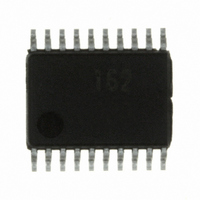
IC R8C MCU FLASH 8K 20SSOP
Manufacturer
Renesas Electronics America
Series
M16C™ M16C/R8C/Tiny/16r
Datasheets
1.R5F211A2SPU0.pdf
(300 pages)
2.R5F21173DSPU0.pdf
(40 pages)
3.R5F21173DSPU0.pdf
(281 pages)
Specifications of R5F21162SP#U0
Core Processor
R8C
Core Size
16-Bit
Speed
20MHz
Connectivity
I²C, SIO, UART/USART
Peripherals
LED, POR, Voltage Detect, WDT
Number Of I /o
13
Program Memory Size
8KB (8K x 8)
Program Memory Type
FLASH
Ram Size
512 x 8
Voltage - Supply (vcc/vdd)
2.7 V ~ 5.5 V
Data Converters
A/D 4x10b
Oscillator Type
Internal
Operating Temperature
-20°C ~ 85°C
Package / Case
20-SSOP
For Use With
R0K521134S000BE - KIT EVAL STARTER FOR R8C/13
Lead Free Status / RoHS Status
Lead free / RoHS Compliant
Eeprom Size
-


R8C/16 Group, R8C/17 Group
Rev.2.10
REJ09B0169-0210
15.3
Figure 15.9
Setting the FS bit in the SAR register to “0” communicates in I
bus Format and Bus Timing. The 1st frame following start condition consists of 8 bits.
(1) I
(2) I
Explanation of Symbol
S
SLA
R/W
A
DATA : Transmit / receive data
P
(a) I
(b) I
2
2
C bus Format
C bus Timing
: Start condition
: Slave address
: Indicates the direction of data transmit / receive
I
: Acknowledge
: Stop condition
2
2
The master device changes the SDA signal from “L” to “H” while the SCL signal is held “H”.
C bus Format (FS=0)
C bus Format(when start condition is retransmitted, FS=0)
The master device changes the SDA signal from “H” to “L” while the SCL signal is held “H”.
Data is transmitted from the slave device to the master device when R/W signal is “1” and from the master device to the slave device when
The receive device sets the SDA signal to “L”.
Jan 19, 2006
2
R/W signal is “0”.
C bus Format
SDA
SCL
S
S
1
1
S
I
2
C bus Format and Bus Timing
SLA
SLA
7
7
1 to 7
SLA
1
1
Page 151 of 254
R/W
R/W
8
1
R/W
1
A
1
A
1
9
A
DATA
DATA
n
n1
1 to 7
m1
DATA
8
A
1
m
A/A
1
9
A
S
1
A/A
1 to 7
1
SLA
7
2
P
1
DATA
C bus format. Figure 15.9 shows the I
1
Transfer Bit Numbers (n=1 to 8)
Transfer Frame Numbers (m=from 1)
8
R/W
1
9
A
Upper : Transfer Bit Numbers (n1, n2=1 to 8)
Lower : Transfer Frame Numbers (m1, m2= from 1
)
A
1
P
15. I
DATA
n2
2
m2
C bus interface (IIC)
A/A
1
P
1
2
C
Related parts for R5F21162SP#U0
Image
Part Number
Description
Manufacturer
Datasheet
Request
R

Part Number:
Description:
KIT STARTER FOR M16C/29
Manufacturer:
Renesas Electronics America
Datasheet:

Part Number:
Description:
KIT STARTER FOR R8C/2D
Manufacturer:
Renesas Electronics America
Datasheet:

Part Number:
Description:
R0K33062P STARTER KIT
Manufacturer:
Renesas Electronics America
Datasheet:

Part Number:
Description:
KIT STARTER FOR R8C/23 E8A
Manufacturer:
Renesas Electronics America
Datasheet:

Part Number:
Description:
KIT STARTER FOR R8C/25
Manufacturer:
Renesas Electronics America
Datasheet:

Part Number:
Description:
KIT STARTER H8S2456 SHARPE DSPLY
Manufacturer:
Renesas Electronics America
Datasheet:

Part Number:
Description:
KIT STARTER FOR R8C38C
Manufacturer:
Renesas Electronics America
Datasheet:

Part Number:
Description:
KIT STARTER FOR R8C35C
Manufacturer:
Renesas Electronics America
Datasheet:

Part Number:
Description:
KIT STARTER FOR R8CL3AC+LCD APPS
Manufacturer:
Renesas Electronics America
Datasheet:
Part Number:
Description:
KIT STARTER FOR RX610
Manufacturer:
Renesas Electronics America
Datasheet:

Part Number:
Description:
KIT STARTER FOR R32C/118
Manufacturer:
Renesas Electronics America
Datasheet:

Part Number:
Description:
KIT DEV RSK-R8C/26-29
Manufacturer:
Renesas Electronics America
Datasheet:

Part Number:
Description:
KIT STARTER FOR SH7124
Manufacturer:
Renesas Electronics America
Datasheet:

Part Number:
Description:
KIT STARTER FOR H8SX/1622
Manufacturer:
Renesas Electronics America
Datasheet:

Part Number:
Description:
KIT DEV FOR SH7203
Manufacturer:
Renesas Electronics America
Datasheet: