R5F21162SP#U0 Renesas Electronics America, R5F21162SP#U0 Datasheet
R5F21162SP#U0
Specifications of R5F21162SP#U0


Related parts for R5F21162SP#U0


R5F21162SP#U0 Summary of contents
Page 1
To our customers, Old Company Name in Catalogs and Other Documents st On April 1 , 2010, NEC Electronics Corporation merged with Renesas Technology Corporation, and Renesas Electronics Corporation took over all the business of both companies. Therefore, although the ...
Page 2
All information included in this document is current as of the date this document is issued. Such information, however, is subject to change without any prior notice. Before purchasing or using any Renesas Electronics products listed herein, please confirm ...
Page 3
R8C/16 Group, 16 R8C/17 Group Hardware Manual RENESAS 16-BIT SINGLE-CHIP MICROCOMPUTER M16C FAMILY / R8C/Tiny SERIES All information contained in these materials, including products and product specifications, represents information on the product at the time of publication and is subject ...
Page 4
Keep safety first in your circuit designs! Renesas Technology Corp. puts the maximum effort into making semiconductor products 1. better and more reliable, but there is always the possibility that trouble may occur with them. Trouble with semiconductors may lead ...
Page 5
How to Use This Manual 1. Introduction This hardware manual provides detailed information on the R8C/16 Group, R8C/17 Group of microcomputers. Users are expected to have basic knowledge of electric circuits, logical circuits and microcomputers. 2. Register Diagram The symbols, ...
Page 6
M16C Family Documents The following documents were prepared for the M16C family. Document Short Sheet Data Sheet Hardware Manual Software Manual Application Note RENESAS TECHNICAL UPDATE Preliminary report about the specification of a product, a document, NOTES: 1. Before ...
Page 7
SFR Page Reference 1. Overview 1.1 Applications .................................................................................................1 1.2 Performance Overview................................................................................2 1.3 Block Diagram .............................................................................................4 1.4 Product Information .....................................................................................5 1.5 Pin Assignments..........................................................................................7 1.6 Pin Description ............................................................................................8 2. Central Processing Unit (CPU) 2.1 Data Registers (R0, R1, R2 and R3).........................................................11 2.2 ...
Page 8
Special Function Register (SFR) 5. Reset 5.1 Hardware Reset ........................................................................................21 5.1.1 When the power supply is stable........................................................21 5.1.2 Power on ............................................................................................21 5.2 Power-On Reset Function .........................................................................23 5.3 Voltage Monitor 1 Reset ...........................................................................24 5.4 Voltage Monitor 2 Reset............................................................................24 5.5 Watchdog ...
Page 9
Normal Operating Mode .....................................................................48 9.4.2 Wait Mode ..........................................................................................49 9.4.3 Stop Mode ..........................................................................................51 9.5 Oscillation Stop Detection Function ..........................................................53 9.5.1 How to Use Oscillation Stop Detection Function ................................53 10. Protection 11. Interrupt 11.1 Interrupt Overview .....................................................................................56 11.1.1 Types of Interrupts..............................................................................56 ...
Page 10
Programmable Waveform Generation Mode....................................105 13.2.3 Programmable One-Shot Generation Mode.....................................108 13.2.4 Programmable Wait One-shot Generation Mode .............................111 13.3 Timer C....................................................................................................115 13.3.1 Input Capture Mode..........................................................................121 13.3.2 Output Compare Mode .....................................................................123 14. Serial Interface 14.1 Clock Synchronous Serial I/O Mode .......................................................130 14.1.1 ...
Page 11
Internal Equivalent Circuit of Analog Input ..............................................180 16.6 Inflow Current Bypass Circuit ..................................................................181 17. Programmable I/O Ports 17.1 Functions of Programmable I/O Ports .....................................................182 17.2 Effect on Peripheral Functions ................................................................182 17.3 Pins Other than Programmable I/O Ports................................................182 17.4 Port ...
Page 12
Watchdog Timer Interrupt.................................................................237 20.2.5 Changing Interrupt Factor.................................................................238 20.2.6 Changing Interrupt Control Register.................................................239 20.3 Clock Generation Circuit .........................................................................240 20.3.1 Oscillation Stop Detection Function..................................................240 20.3.2 Oscillation Circuit Constants.............................................................240 20.4 Timers .....................................................................................................241 20.4.1 Timers X and Z .................................................................................241 20.4.2 Timer X .............................................................................................241 ...
Page 13
SFR Page Reference Address Register 0000h 0001h 0002h 0003h 0004h Processor Mode Register 0 0005h Processor Mode Register 1 0006h System Clock Control Register 0 0007h System Clock Control Register 1 0008h 0009h Address Match Interrupt Enable Register 000Ah Protect ...
Page 14
Address Register 0080h Timer Z Mode Register 0081h 0082h 0083h 0084h Timer Z Waveform Output Control Register 0085h Prescaler Z 0086h Timer Z Secondary 0087h Timer Z Primary 0088h 0089h 008Ah Timer Z Output Control Register 008Bh Timer X Mode ...
Page 15
Address Register 01B0h 01B1h 01B2h 01B3h Flash Memory Control Register 4 01B4h 01B5h Flash Memory Control Register 1 01B6h 01B7h Flash Memory Control Register 0 01B8h 01B9h 01BAh 01BBh 01BCh 01BDh 01BEh 01BFh 0FFFFh Optional Function Select Register NOTES: 1. ...
Page 16
R8C/16 Group, R8C/17 Group SINGLE-CHIP 16-BIT CMOS MICROCOMPUTER 1. Overview This MCU is built using the high-performance silicon gate CMOS process using the R8C/Tiny Series CPU core and is packaged in a 20-pin plastic molded LSSOP. This MCU operates using ...
Page 17
R8C/16 Group, R8C/17 Group 1.2 Performance Overview Table 1.1 lists the Performance Outline of the R8C/16 Group and Table 1.2 lists the Performance Outline of the R8C/17 Group. Table 1.1 Performance Outline of the R8C/16 Group Item CPU Number of ...
Page 18
R8C/16 Group, R8C/17 Group Table 1.2 Performance Outline of the R8C/17 Group Item CPU Number of Basic Instructions Minimum Instruction Execution Time Operating Mode Address Space Memory Capacity Peripheral Port Function LED drive port Timer Serial Interface ...
Page 19
R8C/16 Group, R8C/17 Group 1.3 Block Diagram Figure 1.1 shows a Block Diagram. I/O port Peripheral Function Timer Timer X (8 bits) Timer Z (8 bits) Timer C (16 bits) Watchdog Timer (15 bits) Figure 1.1 Block Diagram Rev.2.10 Jan ...
Page 20
R8C/16 Group, R8C/17 Group 1.4 Product Information Table 1.3 lists the Product Information of R8C/16 Group and Table 1.4 lists the Product Information of R8C/17 Group. Table 1.3 Product Information of R8C/16 Group Type No. Capacity R5F21162SP 8 Kbytes R5F21163SP ...
Page 21
R8C/16 Group, R8C/17 Group Table 1.4 Product Information of R8C/17 Group ROM Capacity Type No. Program ROM R5F21172SP 8 Kbytes R5F21173SP 12 Kbytes R5F21174SP 16 Kbytes R5F21172DSP 8 Kbytes R5F21173DSP 12 Kbytes R5F21174DSP 16 Kbytes Type No ...
Page 22
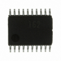
R8C/16 Group, R8C/17 Group 1.5 Pin Assignments Figure 1.4 shows the PLSP0020JB-A Package Pin Assignment (top view). PIN Assignment (top view) P3_5/SCL/CMP1_2 P3_7/CNTR0 RESET (1) XOUT/P4_7 VSS/AVSS XIN/P4_6 VCC MODE P4_5/INT0 P1_7/CNTR00/INT10 Figure 1.4 PLSP0020JB-A Package Pin Assignment (top view) ...
Page 23
R8C/16 Group, R8C/17 Group 1.6 Pin Description Table 1.5 lists the Pin Description and Table 1.6 lists the Pin Name Information by Pin Number. Table 1.5 Pin Description Function Power Supply Input VCC VSS Analog Power Supply AVCC Input AVSS ...
Page 24
R8C/16 Group, R8C/17 Group Table 1.6 Pin Name Information by Pin Number Pin Control Port Number Pin 1 P3_5 2 P3_7 3 RESET 4 XOUT P4_7 5 VSS/AVSS 6 XIN P4_6 7 VCC 8 MODE 9 P4_5 10 P1_7 11 ...
Page 25
R8C/16 Group, R8C/17 Group 2. Central Processing Unit (CPU) Figure 2.1 shows the CPU Register. The CPU contains 13 registers. Of these, R0, R1, R2, R3, A0, A1 and FB comprise a register bank. Two sets of register banks are ...
Page 26
R8C/16 Group, R8C/17 Group 2.1 Data Registers (R0, R1, R2 and R3 16-bit register for transfer, arithmetic and logic operations. The same applies R3. The R0 can be split into high-order bit (R0H) and ...
Page 27
R8C/16 Group, R8C/17 Group 2.8.7 Interrupt Enable Flag (I) The I flag enables a maskable interrupt. An interrupt is disabled when the I flag is set to “0”, and are enabled when the I flag is set to “1”. The ...
Page 28
R8C/16 Group, R8C/17 Group 3. Memory 3.1 R8C/16 Group Figure 3 Memory Map of the R8C/16 group. The R8C/16 group provides 1-Mbyte address space from addresses 00000h to FFFFFh. The internal ROM is allocated lower addresses beginning with ...
Page 29
R8C/16 Group, R8C/17 Group 3.2 R8C/17 Group Figure 3 memory map of the R8C/17 group. The R8C/17 group provides 1-Mbyte address space from addresses 00000h to FFFFFh. The internal ROM (program ROM) is allocated lower addresses beginning with ...
Page 30
R8C/16 Group, R8C/17 Group 4. Special Function Register (SFR) SFR (Special Function Register) is the control register of peripheral functions. Tables 4.1 to 4.4 list the SFR information. Table 4.1 SFR Information(1) Address 0000h 0001h 0002h 0003h 0004h Processor Mode ...
Page 31
R8C/16 Group, R8C/17 Group Table 4.2 SFR Information(2) Address 0040h 0041h 0042h 0043h 0044h 0045h 0046h 0047h 0048h 0049h 004Ah 004Bh 004Ch 004Dh Key Input Interrupt Control Register 004Eh A/D Conversion Interrupt Control Register 004Fh IIC Interrupt Control Register 0050h ...
Page 32
R8C/16 Group, R8C/17 Group Table 4.3 SFR Information(3) Address 0080h Timer Z Mode Register 0081h 0082h 0083h 0084h Timer Z Waveform Output Control Register 0085h Prescaler Z Register 0086h Timer Z Secondary Register 0087h Timer Z Primary Register 0088h 0089h ...
Page 33
R8C/16 Group, R8C/17 Group Table 4.4 SFR Information(4) Address 00C0h A/D Register 00C1h 00C2h 00C3h 00C4h 00C5h 00C6h 00C7h 00C8h 00C9h 00CAh 00CBh 00CCh 00CDh 00CEh 00CFh 00D0h 00D1h 00D2h 00D3h 00D4h A/D Control Register 2 00D5h 00D6h A/D Control ...
Page 34
R8C/16 Group, R8C/17 Group 5. Reset There are resets: hardware reset, power-on reset, voltage monitor 1 reset, voltage monitor 2 reset, watchdog timer reset and software reset. Table 5.1 lists the Reset Name and Factor. Table 5.1 Reset Name and ...
Page 35
R8C/16 Group, R8C/17 Group Table 5.2 shows the Pin Status after Reset, Figure 5.2 shows CPU Register Status after Reset and Figure 5.3 shows Reset Sequence. Table 5.2 Pin Status after Reset Pin Name P1 P3_3 to P3_5, P3_7 P4_5 ...
Page 36
R8C/16 Group, R8C/17 Group 5.1 Hardware Reset A reset is applied using the RESET pin. When an “L” signal is applied to the RESET pin while the power supply voltage meets the recommended performance condition, the pins, CPU and SFR ...
Page 37
R8C/16 Group, R8C/17 Group VCC RESET Figure 5.4 Example of Hardware Reset Circuit and Operation RESET Figure 5.5 Example of Hardware Reset Circuit (Use Example of External Power Supply Voltage Detection Circuit) and Operation Rev.2.10 Jan 19, 2006 Page 22 ...
Page 38
R8C/16 Group, R8C/17 Group 5.2 Power-On Reset Function When the RESET pin is connected to the VCC pin via about 5kΩ pull-up resistor and the VCC pin rises, the function is enabled and the microcomputer resets its pins, CPU, and ...
Page 39
R8C/16 Group, R8C/17 Group 5.3 Voltage Monitor 1 Reset A reset is applied using the built-in voltage detection 1 circuit. The voltage detection 1 circuit monitors the input voltage to the VCC pin. The voltage to monitor is Vdet1. When ...
Page 40
R8C/16 Group, R8C/17 Group 6. Voltage Detection Circuit The voltage detection circuit is a circuit to monitor the input voltage to the VCC pin. This circuit monitors the VCC input voltage by the program. And the voltage monitor 1 reset, ...
Page 41
R8C/16 Group, R8C/17 Group VCC Internal Reference Voltage Figure 6.1 Block Diagram of Voltage Detection Circuit Voltage Detection 1 Circuit VCA26 VCC + Internal - Reference Voltage Voltage detection 1 signal is held “H” when VCA26 bit is set to ...
Page 42
R8C/16 Group, R8C/17 Group Voltage Detection 2 Circuit fRING-S VCA27 VCA13 VCC + Noise Filter Voltage Internal - Detection Reference 2 signal (Filter Width: 200ns) voltage Voltage detection 2 signal is held “H” when VCA27 bit is set to “0” ...
Page 43
R8C/16 Group, R8C/17 Group Voltage Detection Register Symbol VCA1 Bit Symbol — (b2-b0) VCA13 — (b7-b4) NOTES : 1. The VCA13 bit is enabled ...
Page 44
R8C/16 Group, R8C/17 Group Voltage Monitor 1 Circuit Control Register Symbol VW1C Bit Symbol VW1C0 VW1C1 VW1C2 — (b3) VW1F0 VW1F1 VW1C6 VW1C7 NOTES : 1. Set the PRC3 bit in ...
Page 45
R8C/16 Group, R8C/17 Group Voltage Monitor 2 Circuit Control Register Symbol VW2C Bit Symbol VW2C0 VW2C1 VW2C2 VW2C3 VW2F0 VW2F1 VW2C6 VW2C7 NOTES : 1. Set the PRC3 bit in the PRCR ...
Page 46
R8C/16 Group, R8C/17 Group 6.1 Monitoring VCC Input Voltage 6.1.1 Monitoring Vdet1 Vdet1 cannot be monitored. 6.1.2 Monitoring Vdet2 Set the VCA27 bit in the VCA2 register to “1” (voltage detection 2 circuit enabled). After td(E-A) (refer to 19. Electrical ...
Page 47
R8C/16 Group, R8C/17 Group 6.2 Voltage Monitor 1 Reset Table 6.2 lists the Setting Procedure of Voltage Monitor 1 Reset Associated Bit and Figure 6.7 shows the Operating Example of Voltage Monitor 1 Reset. When using the voltage monitor 1 ...
Page 48
R8C/16 Group, R8C/17 Group 6.3 Voltage Monitor 2 Interrupt and Voltage Monitor 2 Reset Table 6.3 lists the Setting Procedure of Voltage Monitor 2 Interrupt and Voltage Monitor 2 Reset Associated Bit. Figure 6.8 shows the Operating Example of Voltage ...
Page 49
R8C/16 Group, R8C/17 Group Vdet2 (Typ. 3.30V) (1) 2.7V VCA13 Bit VW2C2 Bit When the VW2C1 bit is set to “0” (digital filter enabled) Voltage Monitor 2 Interrupt Request (VW2C6=0) Internal Reset Signal (VW2C6=1) VW2C2 Bit When the VW2C1 bit ...
Page 50
R8C/16 Group, R8C/17 Group 7. Processor Mode 7.1 Types of Processor Mode Single-chip mode can be selected as processor mode. Table 7.1 lists Features of Processor Mode. Figure 7.1 shows the PM0 Register and Figure 7.2 shows the PM1 Register. ...
Page 51
R8C/16 Group, R8C/17 Group (1) Processor Mode Register Symbol PM1 Bit Symbol — (b0) — (b1) PM12 — (b6-b3) — (b7) NOTES : 1. Set the PRC1 bit in ...
Page 52
R8C/16 Group, R8C/17 Group 8. Bus During access, the ROM/RAM and SFR vary from bus cycles. Table 8.1 lists Bus Cycles for Access Area of the R8C/16 Group and Table 8.2 lists Bus Cycles for Access Space of the R8C/17 ...
Page 53
R8C/16 Group, R8C/17 Group 9. Clock Generation Circuit The MCU has two on-chip clock generation circuits: • Main clock oscillation circuit • On-chip oscillator (oscillation stop detection function) Table 9.1 lists a Clock Generation Circuit Specification. Figure 9.1 shows a ...
Page 54
R8C/16 Group, R8C/17 Group S Q CM10=1(Stop Mode) R RESET Power-on reset Software reset S Q Interrupt request WAIT R Instruction CM13 XIN XOUT CM13 CM05 CM02, CM05, CM06: Bits in CM0 register CM10, CM13, CM14, CM16, CM17: Bits in ...
Page 55
R8C/16 Group, R8C/17 Group System Clock Control Register Symbol CM0 Bit Symbol — (b1-b0) CM02 — (b3) — (b4) CM05 CM06 — (b7) NOTES : 1. ...
Page 56
R8C/16 Group, R8C/17 Group System Clock Control Register Symbol CM1 Bit Symbol CM10 — (b1) — (b2) CM13 CM14 CM15 CM16 CM17 NOTES : 1. Set the PRC0 bit ...
Page 57
R8C/16 Group, R8C/17 Group Oscillation Stop Detection Register Symbol OCD Bit Symbol OCD0 OCD1 OCD2 OCD3 — (b7-b4) NOTES : 1. Set the PRC0 bit in the PRCR ...
Page 58
R8C/16 Group, R8C/17 Group High-speed On-Chip Oscillator Control Register Symbol HRA0 Bit Symbol HRA00 HRA01 — (b7-b2) NOTES : 1. Set the PRC0 bit in ...
Page 59
R8C/16 Group, R8C/17 Group High-speed On-Chip Oscillator Control Register Symbol HRA1 The frequency of high-speed on-chip oscillator is adjusted w ith bits High-speed on-chip oscillator frequency = 8MHz ...
Page 60
R8C/16 Group, R8C/17 Group The following describes the clocks generated by the clock generation circuit. 9.1 Main Clock This clock is supplied by a main clock oscillation circuit. This clock is used as the clock source for the CPU and ...
Page 61
R8C/16 Group, R8C/17 Group 9.2 On-Chip Oscillator Clock This clock is supplied by an on-chip oscillator. The on-chip oscillator contains a high-speed on-chip oscillator and a low-speed on-chip oscillator. Either an on-chip oscillator clock is selected by the HRA01 bit ...
Page 62
R8C/16 Group, R8C/17 Group 9.3 CPU Clock and Peripheral Function Clock There are two type clocks: a CPU clock to operate the CPU and a peripheral function clock to operate the peripheral functions. Refer to Figure 9.1 Clock Generation Circuit. ...
Page 63
R8C/16 Group, R8C/17 Group 9.4 Power Control There are three power control modes. All modes other than wait and stop modes are referred to as normal operating mode. 9.4.1 Normal Operating Mode Normal operating mode is further separated into four ...
Page 64
R8C/16 Group, R8C/17 Group 9.4.1.1 High-Speed Mode The main clock divided-by-1 (no division) provides the CPU clock. If the CM14 bit is set to “0” (low- speed on-chip oscillator on) or the HRA00 bit in the HRA0 register is set ...
Page 65
R8C/16 Group, R8C/17 Group 9.4.2.4 Exiting Wait Mode The microcomputer exits wait mode by a hardware reset or peripheral function interrupt. When using a hardware reset to exit wait mode, set the ILVL2 to ILVL0 bits for the peripheral function ...
Page 66
R8C/16 Group, R8C/17 Group 9.4.3 Stop Mode Since the oscillator circuits stop in stop mode, the CPU clock and peripheral function clock stop and the CPU and peripheral functions operated by these clocks stop operating. The least power required to ...
Page 67
R8C/16 Group, R8C/17 Group Figure 9.8 shows the State Transition of Power Control. Low-speed On-chip Oscillator Mode High-speed Mode, Middle-speed Mode OCD2=0 CM05=0 CM13=1 High-speed On-chip Oscillator Mode WAIT Interrupt Instruction Wait Mode Figure 9.8 State Transition of Power Control ...
Page 68
R8C/16 Group, R8C/17 Group 9.5 Oscillation Stop Detection Function The oscillation stop detection function is a function to detect the stop of the main clock oscillation circuit. The oscillation stop detection function can be enabled or disabled by the OCD1 ...
Page 69
R8C/16 Group, R8C/17 Group Table 9.6 Determine Interrupt Factor of Oscillation Stop Detection, Watchdog Timer and Voltage Monitor 2 Interrupts Generated Interrupt Factor Oscillation Stop Detection ( (a) or (b) ) Watchdog Timer Voltage Monitor 2 Set OCD1 to OCD0 ...
Page 70
R8C/16 Group, R8C/17 Group 10. Protection Protection function protects important registers from being easily overwritten when a program runs out of control. Figure 10.1 shows the PRCR Register. The following lists the registers protected by the PRCR register. • Registers ...
Page 71
R8C/16 Group, R8C/17 Group 11. Interrupt 11.1 Interrupt Overview 11.1.1 Types of Interrupts Figure 11.1 shows types of Interrupts. Software (Non-Maskable Interrupt) Interrupt Hardware NOTES : 1. Peripheral function interrupts in the microcomputer are used to generate the peripheral interrupt. ...
Page 72
R8C/16 Group, R8C/17 Group 11.1.2 Software Interrupts A software interrupt is generated when an instruction is executed. The software interrupts are non- maskable interrupts. 11.1.2.1 Undefined Instruction Interrupt The undefined instruction interrupt is generated when the UND instruction is executed. ...
Page 73
R8C/16 Group, R8C/17 Group 11.1.3 Special Interrupts Special interrupts are non-maskable interrupts. 11.1.3.1 Watchdog Timer Interrupt The watchdog timer interrupt is generated by the watchdog timer. Reset the watchdog timer after the watchdog timer interrupt is generated. For details, refer ...
Page 74
R8C/16 Group, R8C/17 Group 11.1.5 Interrupts and Interrupt Vector There are 4 bytes in one vector. Set the starting address of interrupt routine in each vector table. When an interrupt request is acknowledged, the CPU branches to the address set ...
Page 75
R8C/16 Group, R8C/17 Group 11.1.5.2 Relocatable Vector Tables The relocatable vector tables occupy 256 bytes from the starting address set in the INTB register. Table 11.2 lists the Relocatable Vector Tables. Table 11.2 Relocatable Vector Tables Interrupt Factor Address (L) ...
Page 76
R8C/16 Group, R8C/17 Group 11.1.6 Interrupt Control The following describes enable/disable the maskable interrupts and set the priority order to acknowledge. The contents explained does not apply to the nonmaskable interrupts. Use the I flag in the FLG register, IPL ...
Page 77
R8C/16 Group, R8C/17 Group INT0 Interrupt Control Register Symbol INT01C Bit Symbol ILVL0 ILVL1 ILVL2 IR POL — (b5) — (b7-b6) NOTES : 1. Only “0” can be w ritten to ...
Page 78
R8C/16 Group, R8C/17 Group 11.1.6.1 I Flag The I flag enables or disables the maskable interrupt. Setting the I flag to “1” (enabled) enables the maskable interrupt. Setting the I flag to “0” (disabled) disables all maskable interrupts. 11.1.6.2 IR ...
Page 79
R8C/16 Group, R8C/17 Group 11.1.6.4 Interrupt Sequence An interrupt sequence is performed between an interrupt request acknowledgement and interrupt routine execution. When an interrupt request is generated while an instruction is executed, the CPU determines its interrupt priority level after ...
Page 80
R8C/16 Group, R8C/17 Group 11.1.6.5 Interrupt Response Time Figure 11.6 shows an Interrupt Response Time. The interrupt response time is the period between an interrupt request generation and the execution of the first instruction in an interrupt routine. An interrupt ...
Page 81
R8C/16 Group, R8C/17 Group 11.1.6.7 Saving a Register In the interrupt sequence, the FLG register and PC are saved to the stack. After 4 high-order bits in the PC and 4 high-order (IPL) and 8 low-order bits in the FLG ...
Page 82
R8C/16 Group, R8C/17 Group 11.1.6.8 Returning from an Interrupt Routine When the REIT instruction is executed at the end of an interrupt routine, the FLG register and PC, which have been saved to the stack, are automatically returned. The program, ...
Page 83
R8C/16 Group, R8C/17 Group 11.1.6.10 Interrupt Priority Judgement Circuit The interrupt priority judgement circuit selects the highest priority interrupt. Figure 11.10 shows the Judgement Circuit of Interrupts Priority Level. Priority Level of Each Interrupt Compare 0 INT3 Timer Z Timer ...
Page 84
R8C/16 Group, R8C/17 Group 11.2 INT Interrupt 11.2.1 INT0 Interrupt The INT0 interrupt is generated by an INT0 input. When using the INT0 interrupt, the INT0EN bit in the INTEN register is set to “1” (enable). The edge polarity is ...
Page 85
R8C/16 Group, R8C/17 Group 11.2.2 INT0 Input Filter The INT0 input contains a digital filter. The sampling clock is selected by the INT0F1 to INT0F0 bits in the INT0F register. The IR bit in the INT0IC register is set to ...
Page 86
R8C/16 Group, R8C/17 Group 11.2.3 INT1 Interrupt The INT1 interrupt is generated by INT1 inputs. The edge polarity is selected by the R0EDG bit in the TXMR register. When the CNTRSEL bit in the UCON register is set to “0”, ...
Page 87
R8C/16 Group, R8C/17 Group 11.2.4 INT3 Interrupt The INT3 interrupt is generated by the INT3 input. Set the TCC07 bit in the TCC0 register to “0” (INT3). When the TCC06 bit in the TCC0 register is set to “0”, the ...
Page 88
R8C/16 Group, R8C/17 Group Timer C Control Register Symbol TCC1 Bit Symbol TCC10 TCC11 TCC12 TCC13 TCC14 TCC15 TCC16 TCC17 NOTES : 1. When the same value from the INT3 2. ...
Page 89
R8C/16 Group, R8C/17 Group 11.3 Key Input Interrupt A key input interrupt request is generated by one of the input edges of the K10 to K13 pins. The key input interrupt can be used as a key-on wake-up function to ...
Page 90
R8C/16 Group, R8C/17 Group (1) Key Input Enable Register Symbol KIEN Bit Symbol KI0EN KI0PL KI1EN KI1PL KI2EN KI2PL KI3EN KI3PL NOTES : 1. The IR bit in the KUPIC register may ...
Page 91
R8C/16 Group, R8C/17 Group 11.4 Address Match Interrupt An address match interrupt request is generated immediately before executing the instruction at the address indicated by the RMADi register (i=0, 1). This interrupt is used for a break function of the ...
Page 92
R8C/16 Group, R8C/17 Group Address Match Interrupt Enable Register Symbol AIER Bit Symbol AIER0 AIER1 — (b7-b2) Address Match Interrupt Register i(i=0,1) (b23) (b19) (b16) (b15 Address setting ...
Page 93
R8C/16 Group, R8C/17 Group 12. Watchdog Timer The watchdog timer is a function to detect when the program is out of control. To use the watchdog timer is recommend for improving reliability of a system. The watchdog timer contains a ...
Page 94
R8C/16 Group, R8C/17 Group Option Function Select Register Symbol OFS Bit Symbol WDTON — (b1) ROMCR ROMCP1 — (b6-b4) CSPROINI NOTES : 1. The OFS register is on ...
Page 95
R8C/16 Group, R8C/17 Group Watchdog Timer Reset Register b7 b0 Symbol WDTR When w riting “00h” before w riting “FFh”, the w atchdog timer is reset. The default value of the w atchdog timer is set to “7FFFh” w hen ...
Page 96
R8C/16 Group, R8C/17 Group 12.1 When Count Source Protection Mode Disabled The count source of the watchdog timer is the CPU clock when count source protection mode is disabled. Table 12.2 lists the Specification of Watchdog Timer (When Count Source ...
Page 97
R8C/16 Group, R8C/17 Group 12.2 When Count Source Protection Mode Enabled The count source of the watchdog timer is the low-speed on-chip oscillator clock when count source protection mode is enabled. If the CPU clock stops when the program is ...
Page 98
R8C/16 Group, R8C/17 Group 13. Timers The microcomputer contains two 8-bit timers with 8-bit prescaler and a 16-bit timer. The two 8-bit timers with the 8-bit prescaler contain Timer X and Timer Z. These timers contain a reload register to ...
Page 99
R8C/16 Group, R8C/17 Group 13.1 Timer X Timer 8-bit timer with an 8-bit prescaler. The prescaler and timer consist of the reload register and counter. The reload register and counter are allocated at the same address. When ...
Page 100
R8C/16 Group, R8C/17 Group Timer X Mode Register Symbol TXMR Bit Symbol TXMOD0 TXMOD1 R0EDG TXS TXOCNT TXMOD2 TXEDG TXUND NOTES : 1. The IR bit in the INT1IC register may be ...
Page 101
R8C/16 Group, R8C/17 Group Prescaler X Register b7 b0 Symbol Timer Mode Pulse Output Mode Event Counter Mode Pulse Width Measurement Mode Pulse Period Measurement Mode Timer X Register b7 b0 Symbol Counts underflow of Prescaler X Timer Count Source ...
Page 102
R8C/16 Group, R8C/17 Group 13.1.1 Timer Mode Timer mode is mode to count the count source which is internally generated (See Table 13.2 Specification of Timer Mode). Figure 13.4 shows the TXMR Register in Timer Mode. Table 13.2 Specification of ...
Page 103
R8C/16 Group, R8C/17 Group 13.1.2 Pulse Output Mode Pulse output mode is mode to count the count source internally generated and outputs the pulse which inverts the polarity from the CNTR0 pin each time the timer underflows (See Table 13.3 ...
Page 104
R8C/16 Group, R8C/17 Group Timer X Mode Register Symbol TXMR Bit Symbol TXMOD0 TXMOD1 R0EDG TXS TXOCNT TXMOD2 TXEDG TXUND NOTES : 1. The IR bit in ...
Page 105
R8C/16 Group, R8C/17 Group 13.1.3 Event Counter Mode Event counter mode is mode to count an external signal which inputs from the INT1/CNTR0 pin (See Table 13.4 Specification of Event Counter Mode). Figure 13.6 shows TXMR Register in Event Counter ...
Page 106
R8C/16 Group, R8C/17 Group Timer X Mode Register Symbol TXMR Bit Symbol TXMOD0 TXMOD1 R0EDG TXS TXOCNT TXMOD2 TXEDG TXUND NOTES : 1. The IR bit ...
Page 107
R8C/16 Group, R8C/17 Group 13.1.4 Pulse Width Measurement Mode Pulse width measurement mode is mode to measure the pulse width of an external signal which inputs from the INT1/CNTR0 pin (See Table 13.5 Specification of Pulse Width Measurement Mode). Figure ...
Page 108
R8C/16 Group, R8C/17 Group Timer X Mode Register Symbol TXMR Bit Symbol TXMOD0 TXMOD1 R0EDG TXS TXOCNT TXMOD2 TXEDG TXUND NOTES : 1. The IR bit ...
Page 109
R8C/16 Group, R8C/17 Group n = high-level: the contents of TX register, low-level: the contents of PREX register FFFFh Count Start n 0000h Set to “1” by program “1” TXS Bit in TXMR Register “0” “1” Measurement Pulse (CNTR0i Pin ...
Page 110
R8C/16 Group, R8C/17 Group 13.1.5 Pulse Period Measurement Mode Pulse period measurement mode is mode to measure the pulse period of an external signal which inputs from the INT1/CNTR0 pin (See Table 13.6 Specification of Pulse Period Measurement Mode). Figure ...
Page 111
R8C/16 Group, R8C/17 Group Timer X Mode Register Symbol TXMR Bit Symbol TXMOD0 TXMOD1 R0EDG TXS TXOCNT TXMOD2 (2) TXEDG (2) TXUND NOTES : 1. The IR bit ...
Page 112
R8C/16 Group, R8C/17 Group Underflow Signal of Prescaler X Set to “1” by program TXS Bit in TXMR “1” Register “0” Starts counting “1” CNTR0i Pin Input “0” Contents of Timer X 0Fh Contents of Read-Out Buffer1 TXEDG Bit in ...
Page 113
R8C/16 Group, R8C/17 Group 13.2 Timer Z Timer 8-bit timer with an 8-bit prescaler. The prescaler and timer consist of the reload register and counter. The reload register and counter are allocated at the same address. Refer ...
Page 114
R8C/16 Group, R8C/17 Group Timer Z Mode Register Symbol TZMR Bit Symbol — (b3-b0) TZMOD0 TZMOD1 TZWC TZS NOTES : 1. Refer to 20.4.3 Tim er Z for ...
Page 115
R8C/16 Group, R8C/17 Group Prescaler Z Register b7 b0 Timer Mode Programmable Waveform Generation Mode Programmable One-Shot Generation Mode Programmable Wait One- Shot Generation Mode Timer Z Secondary Register b7 b0 Timer Mode Programmable Waveform Generation Mode Programmable One-Shot Generation ...
Page 116
R8C/16 Group, R8C/17 Group Timer Z Output Control Register Symbol TZOC Bit Symbol TZOS — (b1) TZOCNT — (b7-b3) NOTES : 1. This bit is set to “0” w hen the ...
Page 117
R8C/16 Group, R8C/17 Group Timer Count Source Setting Register Symbol TCSS Bit Symbol TXCK0 TXCK1 — (b3-b2) TZCK0 TZCK1 — (b7-b6) NOTES : 1. Do not sw itch ...
Page 118
R8C/16 Group, R8C/17 Group 13.2.1 Timer Mode Timer mode is mode to count a count source which is internally generated or Timer X underflow (see Table 13.7 Specification of Timer Mode). The TZSC register is unused in timer mode. Figure ...
Page 119
R8C/16 Group, R8C/17 Group Timer Z Mode Register Symbol TZMR Bit Symbol — (b3-b0) TZMOD0 TZMOD1 TZWC TZS NOTES : 1. When the TZS bit is ...
Page 120
R8C/16 Group, R8C/17 Group 13.2.2 Programmable Waveform Generation Mode Programmable waveform generation mode is mode to invert the signal output from the TZOUT pin each time the counter underflows, while the values in the TZPR and TZSC registers are counted ...
Page 121
R8C/16 Group, R8C/17 Group Timer Z Mode Register Symbol TZMR Bit Symbol — (b3-b0) TZMOD0 TZMOD1 TZWC TZS NOTES : 1. When the TZS bit ...
Page 122
R8C/16 Group, R8C/17 Group “1” TZS Bit in TZMR Register “0” Count Source Prescaler Z Underflow Signal Contents of Timer Z “1” IR Bit in TZIC Register “0” “1” TZOPL Bit in PUM Register “0” “H” TZOUT Pin Output “L” ...
Page 123
R8C/16 Group, R8C/17 Group 13.2.3 Programmable One-Shot Generation Mode Programmable one-shot generation mode is mode to output the one-shot pulse from the TZOUT pin by a program or an external trigger input (input to the INT0 pin). (see Table 13.9 ...
Page 124
R8C/16 Group, R8C/17 Group Timer Z Mode Register Symbol TZMR Bit Symbol — (b3-b0) TZMOD0 TZMOD1 TZWC TZS NOTES : 1. When the TZS bit ...
Page 125
R8C/16 Group, R8C/17 Group "1" TZS Bit in TZMR Register "0" "1" TZOS Bit in TZOC Register "0" Count Source Prescaler Z Underflow Signal "1" INT0 Pin Input "0" Contents of Timer Z "1" IR Bit in TZIC Register "0" ...
Page 126
R8C/16 Group, R8C/17 Group 13.2.4 Programmable Wait One-shot Generation Mode Programmable wait one-shot generation mode is mode to output the one-shot pulse from the TZOUT pin by the external trigger input (input to the INT0 pin) (see Table 13.10 Specification ...
Page 127
R8C/16 Group, R8C/17 Group Table 13.10 Specification of Programmable Wait One-shot Generation Mode Item Count Source Count Operation Wait Time One-Shot Pulse Output Time (n+1)(p+1)/fi Count Start Condition Count Stop Condition Interrupt Request Generation Timing TZOUT Pin Function INT0 Pin ...
Page 128
R8C/16 Group, R8C/17 Group Timer Z Mode Register Symbol TZMR Bit Symbol — (b3-b0) TZMOD0 TZMOD1 TZWC TZS NOTES : 1. When the TZS bit ...
Page 129
R8C/16 Group, R8C/17 Group TZS Bit in TZMR "1" Register "0" TZOS Bit in TZOC "1" Register "0" Count Source Prescaler Z Underflow Signal "1" INT0 Pin Input "0" Contents of Timer Z "1" IR Bit in TZIC Register "0" ...
Page 130
R8C/16 Group, R8C/17 Group 13.3 Timer C Timer 16-bit timer. Figure 13.23 shows the Block Diagram of Timer C. Figure 13.24 shows the Block Diagram of CMP Waveform Generation Unit. Figure 13.25 shows the Block Diagram of ...
Page 131
R8C/16 Group, R8C/17 Group TCC14 TCC15 Compare 0 Interrupt Signal Compare 1 Interrupt Signal TCC16 TCC17 TCC17 to TCC16 H =11b L =10b Reverse =01b TCC15 to TCC14 Reverse =01b L =10b H =11b TCC14 to TCC17: Bits in TCC1 ...
Page 132
R8C/16 Group, R8C/17 Group Timer C Register (b15) (b8 Count the internal count source. “0000h” can be read out by reading w hen the TCC00 bit is set to “0” (count stops) The count value can be ...
Page 133
R8C/16 Group, R8C/17 Group Timer C Control Register Symbol TCC0 Bit Symbol TCC00 TCC01 TCC02 TCC03 TCC04 — (b5) TCC06 TCC07 NOTES : 1. Change this bit w hen the ...
Page 134
R8C/16 Group, R8C/17 Group Timer C Control Register Symbol TCC1 Bit Symbol TCC10 TCC11 TCC12 TCC13 TCC14 TCC15 TCC16 TCC17 NOTES : 1. When the same value from the INT3 2. ...
Page 135
R8C/16 Group, R8C/17 Group Timer C Output Control Register Symbol TCOUT Bit Symbol TCOUT0 TCOUT1 TCOUT2 TCOUT3 TCOUT4 TCOUT5 TCOUT6 TCOUT7 NOTES : 1. Set the bits w hich are not used ...
Page 136
R8C/16 Group, R8C/17 Group 13.3.1 Input Capture Mode Input capture mode is mode to input an edge to the TCIN pin or the fRING128 clock as trigger to latch the timer value and generates an interrupt request. The TCIN input ...
Page 137
R8C/16 Group, R8C/17 Group FFFFh Count Starts 0000h Set to "1" by program “1” TCC00 Bit in TCC0 Register “0” The delay caused by digital filter and one count source cycle delay (max.) Measurement Pulse “1” (TCIN Pin Input) “0” ...
Page 138
R8C/16 Group, R8C/17 Group 13.3.2 Output Compare Mode Output compare mode is mode to generate an interrupt request when the value of the TC register matches the value of the TM0 or TM1 register. Table 13.12 shows Specification of Output ...
Page 139
R8C/16 Group, R8C/17 Group Set value in TM1 register Count start Set value in TM0 register 0000h “1” TCC00 bit in TCC0 register “0” “1” IR bit in CMP0IC register “0” “1” IR bit in CMP1IC register “0” “1” CMP0_0 ...
Page 140
R8C/16 Group, R8C/17 Group 14. Serial Interface Serial interface is configured with one channel: UART0. UART0 has an exclusive timer to generate a transfer clock. Figure 14.1 shows a UART0 Block Diagram. Figure 14.2 shows a UART0 Transmit/Receive Unit. UART0 ...
Page 141
R8C/16 Group, R8C/17 Group 1SP SP PAR RXD0 SP 2SP 0 2SP SP PAR SP 1SP Figure 14.2 UART0 Transmit/Receive Unit Rev.2.10 Jan 19, 2006 Page 126 of 254 REJ09B0169-0210 Clock Synchronous Type PRYE=0 Clock PAR UART (7 bits) Synchronous ...
Page 142
R8C/16 Group, R8C/17 Group UART0 Transmit Buffer Register (b15) (b8 — (b8-b0) — (b15-b9) NOTES : 1. When the transfer data length is 9-bit long, w rite to high-byte data first then low -byte data. 2. Use ...
Page 143
R8C/16 Group, R8C/17 Group UART0 Transmit / Receive Mode Register Symbol U0MR Bit Symbol SMD0 SMD1 SMD2 CKDIR STPS PRY PRYE — (b7) NOTES : 1. Set the PD1_6 bit in ...
Page 144
R8C/16 Group, R8C/17 Group UART0 Transmit / Receive Control Register Symbol U0C1 Bit Symbol — (b7-b4) NOTES : 1. The RI bit is set to “0” w ...
Page 145
R8C/16 Group, R8C/17 Group 14.1 Clock Synchronous Serial I/O Mode The clock synchronous serial I/O mode is mode to transmit and receive data using a transfer clock. Table 14.1 lists the Specification of Clock Synchronous Serial I/O Mode. Table 14.2 ...
Page 146
R8C/16 Group, R8C/17 Group Table 14.2 Registers to Be Used and Settings in Clock Synchronous Serial I/O Mode Register Bit U0TB U0RB OER U0BRG U0MR SMD2 to SMD0 CKDIR U0C0 CLK1 ...
Page 147
R8C/16 Group, R8C/17 Group • Example of Transmit Timing (when internal clock is selected) Transfer Clock "1" TE bit in U0C1 register "0" Set data to U0TB register TI bit in U0C1 "1" register "0" TCLK CLK0 TXD0 D0 D1 ...
Page 148
R8C/16 Group, R8C/17 Group 14.1.1 Polarity Select Function Figure 14.7 shows the Transfer Clock Polarity. Use the CKPOL bit in the U0C0 register to select the transfer clock polarity. • When the CKPOL bit in the U0C0 register = 0 ...
Page 149
R8C/16 Group, R8C/17 Group 14.1.3 Continuous Receive Mode Continuous receive mode is held by setting the U0RRM bit in the UCON register to “1” (enables continuous receive mode). In this mode, reading U0RB register sets the TI bit in the ...
Page 150
R8C/16 Group, R8C/17 Group 14.2 Clock Asynchronous Serial I/O (UART) Mode The UART mode allows transmit and receive data after setting the desired bit rate and transfer data format. Table 14.4 lists the Specification of UART Mode. Table 14.5 lists ...
Page 151
R8C/16 Group, R8C/17 Group Table 14.5 Registers to Be Used and Settings in UART Mode Register Bit U0TB U0RB OER,FER,PER,SUM U0BRG U0MR SMD2 to SMD0 CKDIR STPS PRY, PRYE U0C0 CLK0, ...
Page 152
R8C/16 Group, R8C/17 Group • Transmit Timing When Transfer Data is 8-Bit Long (parity enabled, 1 stop bit) Transfer Clock TE Bit in U0C1 “1” Register “0” Write data to U0TB register TI Bit in U0C1 “1” Register “0” Start ...
Page 153
R8C/16 Group, R8C/17 Group • Receive Timing When Transfer Data is 8-Bit Long (parity disabled, 1 stop bit) Output U0BRG RE Bit in "1" U0C1 Register "0" RXD0 Transfer Clock Receive starts when transfer clock is generated by falling edge ...
Page 154
R8C/16 Group, R8C/17 Group 14.2.2 Bit Rate Divided-by-16 of frequency by the U0BRG register in UART mode is a bit rate. <UART Mode> • When selecting internal clock Setting value to the U0BRG register = • When selecting external clock ...
Page 155
R8C/16 Group, R8C/17 Group 2 15 bus Interface (IIC) 2 The I C bus interface (IIC) is the circuit which is used for a serial communication based on the data transfer 2 format of the Philips I C ...
Page 156
R8C/16 Group, R8C/17 Group Output SCL Control Noise Rejection Circuit Output SDA Control Noise Rejection Circuit Figure 15.1 Block Diagram of IIC Rev.2.10 Jan 19, 2006 Page 141 of 254 REJ09B0169-0210 Transmit / Receive Control Circuit ICDRT Register ICDRS Register ...
Page 157
R8C/16 Group, R8C/17 Group SCL SCL Input SCL Output SDA SCL Input SCL Output (Master) Figure 15.2 External Circuit Connection Example of SCL and SDA Pins Rev.2.10 Jan 19, 2006 Page 142 of 254 REJ09B0169-0210 VCC VCC SCL SCL Input ...
Page 158
R8C/16 Group, R8C/17 Group (6) IIC Bus Control Register Symbol ICCR1 Bit Symbol CKS0 CKS1 CKS2 CKS3 TRS MST RCVD ICE NOTES : 1. Set according to the necessary transfer rate ...
Page 159
R8C/16 Group, R8C/17 Group (5) IIC Bus Control Register Symbol ICCR2 Bit Symbol — (b0) IICRST — (b2) SCLO SDAOP SDAO SCP BBSY NOTES : 1. When w riting to the ...
Page 160
R8C/16 Group, R8C/17 Group (7) IIC Bus Mode Register Symbol ICMR Bit Symbol BC0 BC1 BC2 BCWP — (b4) — (b5) WAIT MLS NOTES : 1. Rew rite betw een transfer ...
Page 161
R8C/16 Group, R8C/17 Group IIC Bus Interrupt Enable Register Symbol ICIER Bit Symbol ACKBT ACKBR ACKE STIE NAKIE RIE TEIE TIE NOTES : 1. An overrun error interrupt request is generated w ...
Page 162
R8C/16 Group, R8C/17 Group (7) IIC Bus Status Register Symbol ICSR Bit Symbol ADZ AAS AL STOP NACKF RDRF TEND TDRE NOTES : 1. Each bit is set to “0” when reading ...
Page 163
R8C/16 Group, R8C/17 Group (1) Slave Address Register Symbol SAR Bit Symbol FS SVA0 SVA1 SVA2 SVA3 SVA4 SVA5 SVA6 1. Refer to 20.6.1 Access of Registers Associated w ith IIC for ...
Page 164
R8C/16 Group, R8C/17 Group 15.1 Transfer Clock When the MST bit in the ICCR1 register is set to “0”, the transfer clock is the external clock input from the SCL pin. When the MST bit in the ICCR1 register is ...
Page 165
R8C/16 Group, R8C/17 Group 15.2 Interrupt Request The interrupt request of the IIC contains 6 types when the I clock synchronous serial format is used. Table 15.3 lists the Interrupt Request of IIC. Since these interrupt requests are allocated at ...
Page 166
R8C/16 Group, R8C/17 Group 2 15 bus Format Setting the FS bit in the SAR register to “0” communicates in I bus Format and Bus Timing. The 1st frame following start condition consists of 8 bits. 2 (1) ...
Page 167
R8C/16 Group, R8C/17 Group 15.3.1 Master Transmit Operation In master transmit mode, the master device outputs the transmit clock and data, and the slave device returns an acknowledge signal. Figure 15.10 and Figure 15.11 show the Operation Timing in Master ...
Page 168
R8C/16 Group, R8C/17 Group SCL 1 (Master Output) SDA (Master Output) SDA (Slave Output) “1” TDRE Bit in ICSR Register “0” “1” TEND Bit in ICSR Register “0” ICDRT Register ICDRS Register Process (2)Instruction of start condition by program generation ...
Page 169
R8C/16 Group, R8C/17 Group 15.3.2 Master Receive Operation In master receive mode, the master device outputs the receive clock, receives data from the slave device, and returns an acknowledge signal. Figure 15.12 and Figure 15.13 show the Operation Timing in ...
Page 170
R8C/16 Group, R8C/17 Group Master Transmit Mode SCL 9 (Master Output) SDA (Master Output) SDA A (Slave Output) “1” TDRE Bit in ICSR Register “0” “1” TEND Bit in ICSR Register “0” “1” TRS Bit in ICCR1 Register “0” “1” ...
Page 171
R8C/16 Group, R8C/17 Group SCL 9 (Master Output) SDA (Master Output) A SDA (Slave Output) “1” RDRF Bit in ICSR Register “0” “1” RCVD Bit in ICCR1 Register “0” Data n-1 ICDRS Register Data n-1 ICDRR Register Process (5)Set RCVD ...
Page 172
R8C/16 Group, R8C/17 Group 15.3.3 Slave Transmit Operation In slave transmit mode, the slave device outputs the transmit data while the master device outputs the receive clock and returns an acknowledge signal. Figure 15.14 and Figure 15.15 show the Operation ...
Page 173
R8C/16 Group, R8C/17 Group Slave Receive Mode SCL (Master Output) SDA (Master Output) SCL (Slave Output) SDA (Slave Output) “1” TDRE Bit in ICSR Register “0” “1” TEND Bit in ICSR Register “0” “1” TRS Bit in ICCR1 Register “0” ...
Page 174
R8C/16 Group, R8C/17 Group SCL 9 (Master Output) SDA A (Master Output) SCL (Slave Output) SDA (Slave Output) “1” TDRE Bit in ICSR Register “0” “1” TEND Bit in ICSR Register “0” “1” TRS Bit in ICCR1 Register “0” Data ...
Page 175
R8C/16 Group, R8C/17 Group 15.3.4 Slave Receive Operation In slave receive mode, the master device outputs the transmit clock and data, and the slave device returns an acknowledge signal. Figure 15.16 and Figure 15.17 show the Operation Timing in Slave ...
Page 176
R8C/16 Group, R8C/17 Group SCL 9 (Master Output) SDA (Master Output) SCL (Slave Output) SDA A (Slave Output) “1” RDRF Bit in ICSR Register “0” ICDRS Register ICDRR Register Process (2) Dummy-read of ICDRR register by program Figure 15.16 Operating ...
Page 177
R8C/16 Group, R8C/17 Group 15.4 Clock Synchronous Serial Format When setting the FS bit in the SAR register to “1”, the clock synchronous serial format is used to communicate. Figure 15.18 shows the Transfer Format of Clock Synchronous Serial Format. ...
Page 178
R8C/16 Group, R8C/17 Group 15.4.1 Transmit Operation In transmit mode, transmit data is output from the SDA pin synchronizing with the fall of the transfer clock. The transfer clock is output when the MST bit in the ICCR1 register is ...
Page 179
R8C/16 Group, R8C/17 Group 15.4.2 Receive Operation In receive mode, data is latched at the rise of the transfer clock. The transfer clock is output when the MST bit in the ICCR1 register is set to “1” and input when ...
Page 180
R8C/16 Group, R8C/17 Group 15.5 Noise Rejection Circuit The state of the SCL and SDA pins are routed through the noise rejection circuit before being latched internally. Figure 15.21 shows the Block Diagram of Noise Rejection Circuit. The noise rejection ...
Page 181
R8C/16 Group, R8C/17 Group 15.6 Bit Synchronous Circuit When setting the IIC in master mode. • When the SCL signal is driven to “L” by the slave device. • Since the “H” period may become shorter while the SCL signal ...
Page 182
R8C/16 Group, R8C/17 Group 15.7 Example of Register Setting Figure 15.23 to Figure 15.26 show the Examples of Register Setting When Using IIC. Read BBSY bit in ICCR2 register No ICCR1 Register ICCR2 Register Write transmit data to ICDRT register ...
Page 183
R8C/16 Group, R8C/17 Group Master Receive Mode TEND Bit ← 0 ICSR Register TRS Bit ← 0 ICCR1 Register TDRE Bit ← 0 ICSR Register ACKBT Bit ← 0 ICIER Register Dummy-read in ICDRR register Read RDRF bit in ICSR ...
Page 184
R8C/16 Group, R8C/17 Group Slave Transmit Mode AAS Bit ← 0 ICSR Register Write transmit data to ICDRT register Read TDRE bit in ICSR register TDRE Yes No Last byte ? Yes Write transmit data to ICDRT register ...
Page 185
R8C/16 Group, R8C/17 Group Slave Receive Mode AAS Bit ← 0 ICSR Register ICIER Register ACKBT Bit ← 0 Dummy-read in ICDRR register Read RDRF bit in ICSR register No RDRF=1 ? Yes Last receive - 1 ? Read ICDRR ...
Page 186
R8C/16 Group, R8C/17 Group 16. A/D Converter The A/D converter consists of one 10-bit successive approximation A/D converter circuit with a capacitive coupling amplifier. The analog input shares the pins with P1_0 to P1_3. Therefore, when using these pins, ensure ...
Page 187
R8C/16 Group, R8C/17 Group AVSS VREF ADCAP=0 Software Trigger Timer Z ADCAP=1 Interrupt Request P1_0/AN8 P1_1/AN9 P1_2/AN10 P1_3/AN11 CH0 to CH2, CKS0 : Bits in ADCON0 register CKS1, VCUT: Bits in ADCON1 register Figure 16.1 Block Diagram of A/D Converter ...
Page 188
R8C/16 Group, R8C/17 Group (1) A/D Control Register Symbol ADCON0 Bit Symbol CH0 CH1 CH2 MD ADGSEL0 ADCAP ADST CKS0 NOTES : 1. If the ADCON0 register is rew ...
Page 189
R8C/16 Group, R8C/17 Group (1) A/D Control Register Symbol ADCON2 Bit Symbol SMP — (b3-b1) — (b7-b4) NOTES : 1. When the ADCON2 register is rew ritten during ...
Page 190
R8C/16 Group, R8C/17 Group 16.1 One-Shot Mode In one-shot mode, the input voltage on one selected pin is A/D converted once. Table 16.2 lists the Specifications of One-Shot Mode. Figure 16.4 shows the ADCON0 and ADCON1 Registers in One-shot Mode. ...
Page 191
R8C/16 Group, R8C/17 Group (1) A/D Control Register Symbol ADCON0 Bit Symbol CH0 CH1 CH2 MD ADGSEL0 ADCAP ADST CKS0 NOTES : 1. If the ADCON0 register is ...
Page 192
R8C/16 Group, R8C/17 Group 16.2 Repeat Mode In repeat mode, the input voltage on one selected pin is A-D converted repeatedly. Table 16.3 lists the Specifications of Repeat Mode. Figure 16.5 shows the ADCON0 and ADCON1 Registers in Repeat Mode. ...
Page 193
R8C/16 Group, R8C/17 Group (1) A/D Control Register Symbol ADCON0 Bit Symbol CH0 CH1 CH2 MD ADGSEL0 ADCAP ADST CKS0 NOTES : 1. If the ADCON0 register is ...
Page 194
R8C/16 Group, R8C/17 Group 16.3 Sample and Hold When the SMP bit in the ADCON2 register is set to “1” (with sample and hold function), A/D conversion rate per pin increases to 28 φ AD cycles for 8-bit resolution or ...
Page 195
R8C/16 Group, R8C/17 Group 16.5 Internal Equivalent Circuit of Analog Input Figure 16.8 shows the Internal Equivalent Circuit of Analog Input. VCC VCC VSS Parasitic Diode ON Resistor Approx. 2k Ω Wiring Resistor Approx. 0.2k Ω AN8 SW1 Parasitic Diode ...
Page 196
R8C/16 Group, R8C/17 Group 16.6 Inflow Current Bypass Circuit Figure 16.9 shows the Configuration of the Inflow Current Bypass Circuit, Figure 16.10 shows the Example of an Inflow Current Bypass Circuit where VCC or More is Applied. OFF Unselected Channel ...
Page 197
R8C/16 Group, R8C/17 Group 17. Programmable I/O Ports Programmable Input/Output ports (hereafter referred to as “I/O ports”) have 13 ports of the P1, P3_3 to P3_5, P3_7, and P4_5. Also, the main clock oscillation circuit is not used, the P4_6 ...
Page 198
R8C/16 Group, R8C/17 Group P1_0 to P1_3 Direction Output from each peripheral function Data Bus Port Latch Input to each peripheral function P1_4 Direction Output from each peripheral function Data Bus Port Latch P1_5 Direction Data Bus Port Latch Input ...
Page 199
R8C/16 Group, R8C/17 Group P1_6, P1_7 Output from each peripheral function Data Bus Port Latch Input to each peripheral function P3_3 Output from each peripheral function Data Bus Input to each peripheral function P3_4, P3_5, P3_7 Output from each peripheral ...
Page 200
R8C/16 Group, R8C/17 Group P4_5 Data Bus Input to each peripheral P4_6/XIN P4_7/XOUT NOTES: 1. When CM05=1, CM10=1, or CM13=0, the clocked inverter is cutoff. 2. When CM10=1 or CM13=0, the feedback resistor is unconnected. 3. When CM05=CM13=1 or CM10=CM13=1, ...