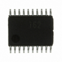
R5F21162SP#U0 Renesas Electronics America, R5F21162SP#U0 Datasheet - Page 186

R5F21162SP#U0
Manufacturer Part Number
R5F21162SP#U0
Description
IC R8C MCU FLASH 8K 20SSOP
Manufacturer
Renesas Electronics America
Series
M16C™ M16C/R8C/Tiny/16r
Datasheets
1.R5F211A2SPU0.pdf
(300 pages)
2.R5F21173DSPU0.pdf
(40 pages)
3.R5F21173DSPU0.pdf
(281 pages)
Specifications of R5F21162SP#U0
Core Processor
R8C
Core Size
16-Bit
Speed
20MHz
Connectivity
I²C, SIO, UART/USART
Peripherals
LED, POR, Voltage Detect, WDT
Number Of I /o
13
Program Memory Size
8KB (8K x 8)
Program Memory Type
FLASH
Ram Size
512 x 8
Voltage - Supply (vcc/vdd)
2.7 V ~ 5.5 V
Data Converters
A/D 4x10b
Oscillator Type
Internal
Operating Temperature
-20°C ~ 85°C
Package / Case
20-SSOP
For Use With
R0K521134S000BE - KIT EVAL STARTER FOR R8C/13
Lead Free Status / RoHS Status
Lead free / RoHS Compliant
Eeprom Size
-
- Current page: 186 of 281
- Download datasheet (4Mb)
R8C/16 Group, R8C/17 Group
Rev.2.10
REJ09B0169-0210
16. A/D Converter
The A/D converter consists of one 10-bit successive approximation A/D converter circuit with a capacitive
coupling amplifier. The analog input shares the pins with P1_0 to P1_3. Therefore, when using these pins,
ensure the corresponding port direction bits are set to “0” (input mode).
When not using the A/D converter, set the VCUT bit in the ADCON1 register to “0” (Vref unconnected), so
that no current will flow from the VREF pin into the resistor ladder, helping to reduce the power consumption
of the chip.
The result of A/D conversion is stored in the AD register.
Table 16.1 lists the Performance of A/D converter. Figure 16.1 shows the Block Diagram of A/D Converter.
Figures 16.2 and 16.3 show the A/D Converter-Associated Registers.
Table 16.1
NOTES:
A/D Conversion Method
Analog Input Voltage
Operating Clock φ AD
Resolution
Absolute Accuracy
Operating Mode
Analog Input Pin
A/D Conversion Start Condition • Software trigger
Conversion Rate Per Pin
1. Analog input voltage does not depend on use of sample and hold function.
2. The frequency of φ AD must be 10 MHz or below.
3. In repeat mode, only 8-bit mode can be used.
Without sample and hold function, the φ AD frequency should be 250 kHz or above.
With the sample and hold function, the φ AD frequency should be 1 MHz or above.
Jan 19, 2006
Item
Performance of A/D converter
(1)
(2)
Page 171 of 254
Successive approximation (with capacitive coupling amplifier)
0V to Vref
4.2V ≤ AVCC ≤ 5.5V f1, f2, f4
2.7V ≤ AVCC < 4.2V f2, f4
8 bit or 10 bit is selectable
AVCC = Vref = 5V
• 8-bit resolution ±2 LSB
• 10-bit resolution ±3 LSB
AVCC = Vref = 3.3 V
• 8-bit resolution ±2 LSB
• 10-bit resolution ±5 LSB
One-shot and repeat modes
4 pins (AN8 to AN11)
• Capture
• Without sample and hold function
• With sample and hold function
Set the ADST bit in the ADCON0 register to “1” (A-D conversion
starts)
Timer Z interrupt request is generated while the ADST bit is set to “1”
8-bit resolution: 49 φ AD cycles, 10-bit resolution: 59 φ AD cycles
8-bit resolution: 28 φ AD cycles, 10-bit resolution: 33 φ AD cycles
(3)
Performance
16. A/D Converter
Related parts for R5F21162SP#U0
Image
Part Number
Description
Manufacturer
Datasheet
Request
R

Part Number:
Description:
KIT STARTER FOR M16C/29
Manufacturer:
Renesas Electronics America
Datasheet:

Part Number:
Description:
KIT STARTER FOR R8C/2D
Manufacturer:
Renesas Electronics America
Datasheet:

Part Number:
Description:
R0K33062P STARTER KIT
Manufacturer:
Renesas Electronics America
Datasheet:

Part Number:
Description:
KIT STARTER FOR R8C/23 E8A
Manufacturer:
Renesas Electronics America
Datasheet:

Part Number:
Description:
KIT STARTER FOR R8C/25
Manufacturer:
Renesas Electronics America
Datasheet:

Part Number:
Description:
KIT STARTER H8S2456 SHARPE DSPLY
Manufacturer:
Renesas Electronics America
Datasheet:

Part Number:
Description:
KIT STARTER FOR R8C38C
Manufacturer:
Renesas Electronics America
Datasheet:

Part Number:
Description:
KIT STARTER FOR R8C35C
Manufacturer:
Renesas Electronics America
Datasheet:

Part Number:
Description:
KIT STARTER FOR R8CL3AC+LCD APPS
Manufacturer:
Renesas Electronics America
Datasheet:

Part Number:
Description:
KIT STARTER FOR RX610
Manufacturer:
Renesas Electronics America
Datasheet:

Part Number:
Description:
KIT STARTER FOR R32C/118
Manufacturer:
Renesas Electronics America
Datasheet:

Part Number:
Description:
KIT DEV RSK-R8C/26-29
Manufacturer:
Renesas Electronics America
Datasheet:

Part Number:
Description:
KIT STARTER FOR SH7124
Manufacturer:
Renesas Electronics America
Datasheet:

Part Number:
Description:
KIT STARTER FOR H8SX/1622
Manufacturer:
Renesas Electronics America
Datasheet:

Part Number:
Description:
KIT DEV FOR SH7203
Manufacturer:
Renesas Electronics America
Datasheet:


