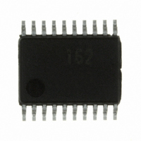
R5F21162SP#U0 Renesas Electronics America, R5F21162SP#U0 Datasheet - Page 191

R5F21162SP#U0
Manufacturer Part Number
R5F21162SP#U0
Description
IC R8C MCU FLASH 8K 20SSOP
Manufacturer
Renesas Electronics America
Series
M16C™ M16C/R8C/Tiny/16r
Datasheets
1.R5F211A2SPU0.pdf
(300 pages)
2.R5F21173DSPU0.pdf
(40 pages)
3.R5F21173DSPU0.pdf
(281 pages)
Specifications of R5F21162SP#U0
Core Processor
R8C
Core Size
16-Bit
Speed
20MHz
Connectivity
I²C, SIO, UART/USART
Peripherals
LED, POR, Voltage Detect, WDT
Number Of I /o
13
Program Memory Size
8KB (8K x 8)
Program Memory Type
FLASH
Ram Size
512 x 8
Voltage - Supply (vcc/vdd)
2.7 V ~ 5.5 V
Data Converters
A/D 4x10b
Oscillator Type
Internal
Operating Temperature
-20°C ~ 85°C
Package / Case
20-SSOP
For Use With
R0K521134S000BE - KIT EVAL STARTER FOR R8C/13
Lead Free Status / RoHS Status
Lead free / RoHS Compliant
Eeprom Size
-
- Current page: 191 of 281
- Download datasheet (4Mb)
R8C/16 Group, R8C/17 Group
Rev.2.10
REJ09B0169-0210
Figure 16.4
A/D Control Register 0
A/D Control Register 1
b7 b6 b5 b4
NOTES :
b7 b6 b5 b4
NOTES :
0 0 1
1.
2.
3.
4.
1.
2. When the VCUT bit is set to “1”(connected) from “0” (not connected), w ait for 1µs or more before starting
If the ADCON0 register is rew ritten during A/D conversion, the conversion result is indeterminate.
CH0 to CH2 bits are enabled w hen the ADGSEL0 bit is set to “1”. After setting the ADGSEL0 bit to “1”, w rite to the
CH0 to CH2 bits.
When changing A/D operation mode, set the analog input pin again.
Set øAD frequency to 10MHz or below .
If the ADCON1 register is rew ritten during A/D conversion, the conversion result is indeterminate.
A/D conversion.
Jan 19, 2006
1 0
b3 b2 b1 b0
b3 b2
1
0 0
ADCON0 and ADCON1 Registers in One-shot Mode
b1 b0
0
Bit Symbol
Bit Symbol
ADGSEL0
ADCON0
ADCON1
ADCAP
(b2-b0)
(b6-b7)
Symbol
Symbol
(1)
(1)
ADST
CKS0
CKS1
VCUT
BITS
CH0
CH1
CH2
MD
Page 176 of 254
—
—
Analog Input Pin Select
Bit
A/D Operation Mode Select
Bit
A/D Input Group Select Bit
A/D Conversion Automatic
Start Bit
A/D Conversion Start Flag
Frequency Select Bit 0
Reserved Bit
8/10-bit Mode Select Bit
Frequency Select Bit 1
Vref Connect Bit
Reserved Bit
(2)
(3)
Address
Bit Name
Address
Bit Name
00D6h
00D7h
(2)
b2 b1 b0
1 0 0 : AN8
1 0 1 : AN9
1 1 0 : AN10
1 1 1 : AN11
Other than above : Do not set
0 : One-shot mode
0 : Disabled
1 : Enabled (AN8 to AN11)
0 : Starts in softw are trigger (ADST bit)
1 : Starts in capture (requests Timer Z interrupt)
0 : Disables A/D conversion
1 : Starts A/D conversion
[When CKS1 in ADCON1 register = 0]
0 : Select f4
1 : Select f2
[When CKS1 in ADCON1 register = 1]
0 : Select f1
1 : Do not set
Set to “0”
0 : 8-bit mode
1 : 10-bit mode
Refer to a description of the CKS0 bit in the
ADCON0 register function
1 : Vref connected
Set to “0”
(4)
After Reset
00000XXXb
After Reset
Function
Function
00h
16. A/D Converter
RW
RW
RW
RW
RW
RW
RW
RW
RW
RW
RW
RW
RW
RW
RW
Related parts for R5F21162SP#U0
Image
Part Number
Description
Manufacturer
Datasheet
Request
R

Part Number:
Description:
KIT STARTER FOR M16C/29
Manufacturer:
Renesas Electronics America
Datasheet:

Part Number:
Description:
KIT STARTER FOR R8C/2D
Manufacturer:
Renesas Electronics America
Datasheet:

Part Number:
Description:
R0K33062P STARTER KIT
Manufacturer:
Renesas Electronics America
Datasheet:

Part Number:
Description:
KIT STARTER FOR R8C/23 E8A
Manufacturer:
Renesas Electronics America
Datasheet:

Part Number:
Description:
KIT STARTER FOR R8C/25
Manufacturer:
Renesas Electronics America
Datasheet:

Part Number:
Description:
KIT STARTER H8S2456 SHARPE DSPLY
Manufacturer:
Renesas Electronics America
Datasheet:

Part Number:
Description:
KIT STARTER FOR R8C38C
Manufacturer:
Renesas Electronics America
Datasheet:

Part Number:
Description:
KIT STARTER FOR R8C35C
Manufacturer:
Renesas Electronics America
Datasheet:

Part Number:
Description:
KIT STARTER FOR R8CL3AC+LCD APPS
Manufacturer:
Renesas Electronics America
Datasheet:

Part Number:
Description:
KIT STARTER FOR RX610
Manufacturer:
Renesas Electronics America
Datasheet:

Part Number:
Description:
KIT STARTER FOR R32C/118
Manufacturer:
Renesas Electronics America
Datasheet:

Part Number:
Description:
KIT DEV RSK-R8C/26-29
Manufacturer:
Renesas Electronics America
Datasheet:

Part Number:
Description:
KIT STARTER FOR SH7124
Manufacturer:
Renesas Electronics America
Datasheet:

Part Number:
Description:
KIT STARTER FOR H8SX/1622
Manufacturer:
Renesas Electronics America
Datasheet:

Part Number:
Description:
KIT DEV FOR SH7203
Manufacturer:
Renesas Electronics America
Datasheet:


