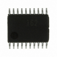
R5F21162SP#U0 Renesas Electronics America, R5F21162SP#U0 Datasheet - Page 230

R5F21162SP#U0
Manufacturer Part Number
R5F21162SP#U0
Description
IC R8C MCU FLASH 8K 20SSOP
Manufacturer
Renesas Electronics America
Series
M16C™ M16C/R8C/Tiny/16r
Datasheets
1.R5F211A2SPU0.pdf
(300 pages)
2.R5F21173DSPU0.pdf
(40 pages)
3.R5F21173DSPU0.pdf
(281 pages)
Specifications of R5F21162SP#U0
Core Processor
R8C
Core Size
16-Bit
Speed
20MHz
Connectivity
I²C, SIO, UART/USART
Peripherals
LED, POR, Voltage Detect, WDT
Number Of I /o
13
Program Memory Size
8KB (8K x 8)
Program Memory Type
FLASH
Ram Size
512 x 8
Voltage - Supply (vcc/vdd)
2.7 V ~ 5.5 V
Data Converters
A/D 4x10b
Oscillator Type
Internal
Operating Temperature
-20°C ~ 85°C
Package / Case
20-SSOP
For Use With
R0K521134S000BE - KIT EVAL STARTER FOR R8C/13
Lead Free Status / RoHS Status
Lead free / RoHS Compliant
Eeprom Size
-
- Current page: 230 of 281
- Download datasheet (4Mb)
R8C/16 Group, R8C/17 Group
Rev.2.10
REJ09B0169-0210
18.5
18.5.1
Table 18.7
VCC,VSS
RESET
P4_6/XIN
P4_7/XOUT
AVCC, AVSS
P1_0 to P1_7
VREF
P3_3 to P3_5
MODE
P3_7
P4_5
In standard serial I/O mode, the user ROM area can be rewritten while the microcomputer is mounted
on-board by using a serial programmer which is applicable for this microcomputer.
Standard serial I/O mode is used to connect with a serial writer using a special clock asynchronous serial
I/O.
There are three types of Standard serial I/O modes:
This microcomputer uses Standard serial I/O mode 2 and Standard serial I/O mode 3.
Refer to Appendix 2. Connecting Example between Serial Writer and On-Chip Debugging
Emulator. Contact the manufacturer of your serial programmer for serial programmer. Refer to the
user’s manual of your serial programmer for details on how to use it.
Table 18.7 lists the Pin Functions (Flash Memory Standard Serial I/O Mode 2), Table 18.8 lists the Pin
Functions (Flash Memory Standard Serial I/O Mode 3). Figure 18.15 show Pin Connections for Standard
Serial I/O Mode 3.
After processing the pins shown in Table 18.8 and rewriting a flash memory using a writer, apply “H” to
the MODE pin and reset a hardware if a program is operated on the flash memory in single-chip mode.
•
•
•
The ID code check function determines whether the ID codes sent from the serial programmer and
those written in the flash memory match (refer to 18.3 Functions To Prevent Flash Memory from
Rewriting ).
Standard serial I/O mode 1 .......... Clock synchronous serial I/O used to connect with a serial
Standard serial I/O mode 2 .......... Clock asynchronous serial I/O used to connect with a serial
Standard serial I/O mode 3 .......... Special clock asynchronous serial I/O used to connect with a serial
Pin
Standard Serial I/O Mode
Jan 19, 2006
ID Code Check Function
Pin Functions (Flash Memory Standard Serial I/O Mode 2)
Power input
Reset input
P4_6 input/clock input
P4_7 input/clock output
Analog power supply input I
Input port P1
Reference voltage input
Input port P3
MODE
TXD output
RXD input
Page 215 of 254
Name
programmer
programmer
programmer
I
I
I/O
I
I
I
I/O Input “L”.
O
I
I/O
Apply the voltage guaranteed for program and erase to
VCC pin and 0V to VSS pin.
Reset input pin.
Connect ceramic resonator or crystal oscillator
between XIN and XOUT pins.
Connect AVSS to VSS and AVCC to VCC, respectively.
Input “H” or “L” level signal or leave the pin open.
Reference voltage input pin to A/D converter.
Input “H” or “L” level signal or leave the pin open.
Serial data output pin.
Serial data input pin.
Description
18. Flash Memory Version
Related parts for R5F21162SP#U0
Image
Part Number
Description
Manufacturer
Datasheet
Request
R

Part Number:
Description:
KIT STARTER FOR M16C/29
Manufacturer:
Renesas Electronics America
Datasheet:

Part Number:
Description:
KIT STARTER FOR R8C/2D
Manufacturer:
Renesas Electronics America
Datasheet:

Part Number:
Description:
R0K33062P STARTER KIT
Manufacturer:
Renesas Electronics America
Datasheet:

Part Number:
Description:
KIT STARTER FOR R8C/23 E8A
Manufacturer:
Renesas Electronics America
Datasheet:

Part Number:
Description:
KIT STARTER FOR R8C/25
Manufacturer:
Renesas Electronics America
Datasheet:

Part Number:
Description:
KIT STARTER H8S2456 SHARPE DSPLY
Manufacturer:
Renesas Electronics America
Datasheet:

Part Number:
Description:
KIT STARTER FOR R8C38C
Manufacturer:
Renesas Electronics America
Datasheet:

Part Number:
Description:
KIT STARTER FOR R8C35C
Manufacturer:
Renesas Electronics America
Datasheet:

Part Number:
Description:
KIT STARTER FOR R8CL3AC+LCD APPS
Manufacturer:
Renesas Electronics America
Datasheet:

Part Number:
Description:
KIT STARTER FOR RX610
Manufacturer:
Renesas Electronics America
Datasheet:

Part Number:
Description:
KIT STARTER FOR R32C/118
Manufacturer:
Renesas Electronics America
Datasheet:

Part Number:
Description:
KIT DEV RSK-R8C/26-29
Manufacturer:
Renesas Electronics America
Datasheet:

Part Number:
Description:
KIT STARTER FOR SH7124
Manufacturer:
Renesas Electronics America
Datasheet:

Part Number:
Description:
KIT STARTER FOR H8SX/1622
Manufacturer:
Renesas Electronics America
Datasheet:

Part Number:
Description:
KIT DEV FOR SH7203
Manufacturer:
Renesas Electronics America
Datasheet:


