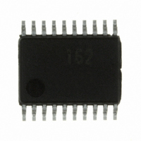
R5F21162SP#U0 Renesas Electronics America, R5F21162SP#U0 Datasheet - Page 276

R5F21162SP#U0
Manufacturer Part Number
R5F21162SP#U0
Description
IC R8C MCU FLASH 8K 20SSOP
Manufacturer
Renesas Electronics America
Series
M16C™ M16C/R8C/Tiny/16r
Datasheets
1.R5F211A2SPU0.pdf
(300 pages)
2.R5F21173DSPU0.pdf
(40 pages)
3.R5F21173DSPU0.pdf
(281 pages)
Specifications of R5F21162SP#U0
Core Processor
R8C
Core Size
16-Bit
Speed
20MHz
Connectivity
I²C, SIO, UART/USART
Peripherals
LED, POR, Voltage Detect, WDT
Number Of I /o
13
Program Memory Size
8KB (8K x 8)
Program Memory Type
FLASH
Ram Size
512 x 8
Voltage - Supply (vcc/vdd)
2.7 V ~ 5.5 V
Data Converters
A/D 4x10b
Oscillator Type
Internal
Operating Temperature
-20°C ~ 85°C
Package / Case
20-SSOP
For Use With
R0K521134S000BE - KIT EVAL STARTER FOR R8C/13
Lead Free Status / RoHS Status
Lead free / RoHS Compliant
Eeprom Size
-
- Current page: 276 of 281
- Download datasheet (4Mb)
Rev.
2.00
REVISION HISTORY
Jan 12, 2006
Date
90, 92, 95 Table 13.4 Specification of Event Counter Mode,
108, 112 Table 13.9 Specification of Programmable One-Shot Generation Mode,
Page
103
116
123
124
87
88
98
Table 13.2 Specification of Timer Mode;
• “INT1/CNTR0 Signal Pin Function” → “INT10/CNTR00, INT11/CNTR01
• “ • When writing ... registers (the data is transferred to the counter when
Table 13.3 Specification of Pulse Output Mode;
• “INT1/CNTR0 Signal Pin Function” → “INT10/CNTR00 Pin Function”
• “ • When writing ... registers (the data is transferred to the counter when
• NOTE1 added
Table 13.5 Specification of Pulse Width Measurement Mode,
Table 13.6 Specification of Pulse Period Measurement Mode;
• “INT1/CNTR0 Signal Pin Function” → “INT10/CNTR00, INT11/CNTR01
• “ • When writing ... registers (the data is transferred to the counter when
Figure 13.11 Block Diagram of Timer Z;
Table 13.7 Specification of Timer Mode;
Table 13.10 Programmable Wait One-Shot Generation Mode Specifications;
Figure 13.25 Block Diagram of CMP Waveform Output Unit revised
Table 13.12 Specification of Output Compare Mode NOTE1 revised
Figure 13.31 Operating Example of Timer C in Output Compare Mode
revised
Pin Function” revised
the following count source is input).” →
“ • When writing ... registers at the following count source input and the
data is transferred to the counter at the second count source input and
the count re-starts at the third count source input.” revised
revised
the following count source is input).” →
“ • When writing ... registers at the following count source input and the
data is transferred to the counter at the second count source input and
the count re-starts at the third count source input.” revised
Pin Function” revised
the following count source is input).” →
“ • When writing ... registers at the following count source input and the
data is transferred to the counter at the second count source input and
the count re-starts at the third count source input.” revised
“Peripheral Data Bus” → “Data Bus” revised
“ • When writing ... registers (the data is transferred to the counter
when the following count source is input) while the TZWC bit is set to
“0” (writing to the reload register and counter simultaneously). ” →
“ • When writing ... registers at the following count source input and the
data is transferred to the counter at the second count source input and
the count re-starts at the third count source input.” revised
Count Operation; “ • When a count completes, ...” → “ • When a count
stops, ...” revised
R8C/16 Group, R8C/17 Group Hardware
C - 7
Description
Summary
Related parts for R5F21162SP#U0
Image
Part Number
Description
Manufacturer
Datasheet
Request
R

Part Number:
Description:
KIT STARTER FOR M16C/29
Manufacturer:
Renesas Electronics America
Datasheet:

Part Number:
Description:
KIT STARTER FOR R8C/2D
Manufacturer:
Renesas Electronics America
Datasheet:

Part Number:
Description:
R0K33062P STARTER KIT
Manufacturer:
Renesas Electronics America
Datasheet:

Part Number:
Description:
KIT STARTER FOR R8C/23 E8A
Manufacturer:
Renesas Electronics America
Datasheet:

Part Number:
Description:
KIT STARTER FOR R8C/25
Manufacturer:
Renesas Electronics America
Datasheet:

Part Number:
Description:
KIT STARTER H8S2456 SHARPE DSPLY
Manufacturer:
Renesas Electronics America
Datasheet:

Part Number:
Description:
KIT STARTER FOR R8C38C
Manufacturer:
Renesas Electronics America
Datasheet:

Part Number:
Description:
KIT STARTER FOR R8C35C
Manufacturer:
Renesas Electronics America
Datasheet:

Part Number:
Description:
KIT STARTER FOR R8CL3AC+LCD APPS
Manufacturer:
Renesas Electronics America
Datasheet:

Part Number:
Description:
KIT STARTER FOR RX610
Manufacturer:
Renesas Electronics America
Datasheet:

Part Number:
Description:
KIT STARTER FOR R32C/118
Manufacturer:
Renesas Electronics America
Datasheet:

Part Number:
Description:
KIT DEV RSK-R8C/26-29
Manufacturer:
Renesas Electronics America
Datasheet:

Part Number:
Description:
KIT STARTER FOR SH7124
Manufacturer:
Renesas Electronics America
Datasheet:

Part Number:
Description:
KIT STARTER FOR H8SX/1622
Manufacturer:
Renesas Electronics America
Datasheet:

Part Number:
Description:
KIT DEV FOR SH7203
Manufacturer:
Renesas Electronics America
Datasheet:


