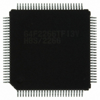
DF2266TF13V Renesas Electronics America, DF2266TF13V Datasheet - Page 95

DF2266TF13V
Manufacturer Part Number
DF2266TF13V
Description
IC H8S/2266 MCU FLASH 100-TQFP
Manufacturer
Renesas Electronics America
Series
H8® H8S/2200r
Datasheet
1.DF2266TF20V.pdf
(712 pages)
Specifications of DF2266TF13V
Core Processor
H8S/2000
Core Size
16-Bit
Speed
13MHz
Connectivity
I²C, SCI, SmartCard
Peripherals
LCD, POR, PWM, WDT
Number Of I /o
67
Program Memory Size
128KB (128K x 8)
Program Memory Type
FLASH
Ram Size
8K x 8
Voltage - Supply (vcc/vdd)
3 V ~ 5.5 V
Data Converters
A/D 10x10b
Oscillator Type
Internal
Operating Temperature
-20°C ~ 75°C
Package / Case
100-TQFP, 100-VQFP
Lead Free Status / RoHS Status
Lead free / RoHS Compliant
Eeprom Size
-
- Current page: 95 of 712
- Download datasheet (5Mb)
2.7.6
The instruction contains 8-bit (#xx:8), 16-bit (#xx:16), or 32-bit (#xx:32) immediate data as an
operand.
The ADDS, SUBS, INC and DEC instructions contain immediate data implicitly. Some bit
manipulation instructions contain 3-bit immediate data in the instruction code, specifying a bit
number. The TRAPA instruction contains 2-bit immediate data in its instruction code, specifying a
vector address.
2.7.7
the instruction is sign-extended and added to the 24-bit PC contents to generate a branch address.
Only the lower 24 bits of this branch address are valid; the upper 8 bits are all assumed to be 0
(H'00). The PC value to which the displacement is added is the address of the first byte of the next
instruction, so the possible branching range is –126 to +128 bytes (–63 to +64 words) or –32766 to
+32768 bytes (–16383 to +16384 words) from the branch instruction. The resulting value should
be an even number.
2.7.8
This mode can be used by the JMP and JSR instructions. The instruction code contains an 8-bit
absolute address specifying a memory operand. This memory operand contains a branch address.
The upper bits of the absolute address are all assumed to be 0, so the address range is 0 to 255
(H'0000 to H'00FF in normal mode * , H'000000 to H'0000FF in advanced mode). In normal mode,
the memory operand is a word operand and the branch address is 16 bits long. In advanced mode,
the memory operand is a longword operand, the first byte of which is assumed to be 0 (H'00).
Note that the first part of the address range is also the exception vector area. For further details,
refer to section 4, Exception Handling.
If an odd address is specified in word or longword memory access, or as a branch address, the
least significant bit is regarded as 0, causing data to be accessed or instruction code to be fetched
at the address preceding the specified address. (For further information, see section 2.5.2, Memory
Data Formats.)
Note: * Normal mode is not available in this LSI.
This mode is used in the Bcc and BSR instructions. An 8-bit or 16-bit displacement contained in
Immediate⎯#xx:8, #xx:16, or #xx:32
Program-Counter Relative⎯@(d:8, PC) or @(d:16, PC)
Memory Indirect⎯@@aa:8
Rev. 5.00 Sep. 01, 2009 Page 43 of 656
REJ09B0071-0500
Section 2 CPU
Related parts for DF2266TF13V
Image
Part Number
Description
Manufacturer
Datasheet
Request
R

Part Number:
Description:
CONN SOCKET 2POS 7.92MM WHITE
Manufacturer:
Hirose Electric Co Ltd
Datasheet:

Part Number:
Description:
CONN SOCKET 4POS 7.92MM WHITE
Manufacturer:
Hirose Electric Co Ltd
Datasheet:

Part Number:
Description:
CONN SOCKET 5POS 7.92MM WHITE
Manufacturer:
Hirose Electric Co Ltd
Datasheet:

Part Number:
Description:
CONN SOCKET 3POS 7.92MM WHITE
Manufacturer:
Hirose Electric Co Ltd
Datasheet:

Part Number:
Description:
CONN SOCKET 5POS 7.92MM WHITE
Manufacturer:
Hirose Electric Co Ltd
Datasheet:

Part Number:
Description:
CONN SOCKET 2POS 7.92MM WHITE
Manufacturer:
Hirose Electric Co Ltd
Datasheet:

Part Number:
Description:
CONN SOCKET 3POS 7.92MM WHITE
Manufacturer:
Hirose Electric Co Ltd
Datasheet:

Part Number:
Description:
CONN SOCKET 4POS 7.92MM WHITE
Manufacturer:
Hirose Electric Co Ltd
Datasheet:

Part Number:
Description:
CONN HEADER 2POS 7.92MM R/A TIN
Manufacturer:
Hirose Electric Co Ltd
Datasheet:

Part Number:
Description:
CONN HEADER 4POS 7.92MM R/A TIN
Manufacturer:
Hirose Electric Co Ltd
Datasheet:

Part Number:
Description:
KIT STARTER FOR M16C/29
Manufacturer:
Renesas Electronics America
Datasheet:

Part Number:
Description:
KIT STARTER FOR R8C/2D
Manufacturer:
Renesas Electronics America
Datasheet:

Part Number:
Description:
R0K33062P STARTER KIT
Manufacturer:
Renesas Electronics America
Datasheet:

Part Number:
Description:
KIT STARTER FOR R8C/23 E8A
Manufacturer:
Renesas Electronics America
Datasheet:

Part Number:
Description:
KIT STARTER FOR R8C/25
Manufacturer:
Renesas Electronics America
Datasheet:


