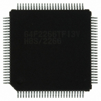
DF2266TF13V Renesas Electronics America, DF2266TF13V Datasheet - Page 591

DF2266TF13V
Manufacturer Part Number
DF2266TF13V
Description
IC H8S/2266 MCU FLASH 100-TQFP
Manufacturer
Renesas Electronics America
Series
H8® H8S/2200r
Datasheet
1.DF2266TF20V.pdf
(712 pages)
Specifications of DF2266TF13V
Core Processor
H8S/2000
Core Size
16-Bit
Speed
13MHz
Connectivity
I²C, SCI, SmartCard
Peripherals
LCD, POR, PWM, WDT
Number Of I /o
67
Program Memory Size
128KB (128K x 8)
Program Memory Type
FLASH
Ram Size
8K x 8
Voltage - Supply (vcc/vdd)
3 V ~ 5.5 V
Data Converters
A/D 10x10b
Oscillator Type
Internal
Operating Temperature
-20°C ~ 75°C
Package / Case
100-TQFP, 100-VQFP
Lead Free Status / RoHS Status
Lead free / RoHS Compliant
Eeprom Size
-
- Current page: 591 of 712
- Download datasheet (5Mb)
This LSI has an on-chip clock pulse generator that generates the system clock (φ), the bus master
clock, and internal clocks. The clock pulse generator consists of an oscillator, duty adjustment
circuit, clock selection circuit, medium-speed clock divider, bus master clock selection circuit,
subclock oscillator, and wave formation circuit. A block diagram of the clock pulse generator is
shown in figure 21.1.
Frequency changes are performed by software by settings in the low-power control register
(LPWRCR) and system clock control register (SCKCR).
CPG0501B_000020020700
EXTAL
XTAL
OSC1
OSC2
Legend:
LPWRCR:
SCKCR:
Low-power control register
System clock control register
oscillator
Subclock
oscillator
System
clock
Figure 21.1 Block Diagram of Clock Pulse Generator
Section 21 Clock Pulse Generator
WDT_1, TMR4, LCD count clock
Generation
adjustment
LPWRCR
Waveform
Circuit
circuit
Duty
RFCUT
φ
SUB
selection
circuit
Clock
Rev. 5.00 Sep. 01, 2009 Page 539 of 656
clock divider
Medium-
speed
peripheral modules
Section 21 Clock Pulse Generator
Internal clock to
Internal
clock φ
φ/2 to
φ/32
selection
REJ09B0071-0500
SCKCR
master
circuit
clock
Bus
Bus master clock
to CPU and DTC
SCK2 to SCK0
Related parts for DF2266TF13V
Image
Part Number
Description
Manufacturer
Datasheet
Request
R

Part Number:
Description:
CONN SOCKET 2POS 7.92MM WHITE
Manufacturer:
Hirose Electric Co Ltd
Datasheet:

Part Number:
Description:
CONN SOCKET 4POS 7.92MM WHITE
Manufacturer:
Hirose Electric Co Ltd
Datasheet:

Part Number:
Description:
CONN SOCKET 5POS 7.92MM WHITE
Manufacturer:
Hirose Electric Co Ltd
Datasheet:

Part Number:
Description:
CONN SOCKET 3POS 7.92MM WHITE
Manufacturer:
Hirose Electric Co Ltd
Datasheet:

Part Number:
Description:
CONN SOCKET 5POS 7.92MM WHITE
Manufacturer:
Hirose Electric Co Ltd
Datasheet:

Part Number:
Description:
CONN SOCKET 2POS 7.92MM WHITE
Manufacturer:
Hirose Electric Co Ltd
Datasheet:

Part Number:
Description:
CONN SOCKET 3POS 7.92MM WHITE
Manufacturer:
Hirose Electric Co Ltd
Datasheet:

Part Number:
Description:
CONN SOCKET 4POS 7.92MM WHITE
Manufacturer:
Hirose Electric Co Ltd
Datasheet:

Part Number:
Description:
CONN HEADER 2POS 7.92MM R/A TIN
Manufacturer:
Hirose Electric Co Ltd
Datasheet:

Part Number:
Description:
CONN HEADER 4POS 7.92MM R/A TIN
Manufacturer:
Hirose Electric Co Ltd
Datasheet:

Part Number:
Description:
KIT STARTER FOR M16C/29
Manufacturer:
Renesas Electronics America
Datasheet:

Part Number:
Description:
KIT STARTER FOR R8C/2D
Manufacturer:
Renesas Electronics America
Datasheet:

Part Number:
Description:
R0K33062P STARTER KIT
Manufacturer:
Renesas Electronics America
Datasheet:

Part Number:
Description:
KIT STARTER FOR R8C/23 E8A
Manufacturer:
Renesas Electronics America
Datasheet:

Part Number:
Description:
KIT STARTER FOR R8C/25
Manufacturer:
Renesas Electronics America
Datasheet:


