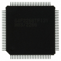
DF2266TF13V Renesas Electronics America, DF2266TF13V Datasheet - Page 281

DF2266TF13V
Manufacturer Part Number
DF2266TF13V
Description
IC H8S/2266 MCU FLASH 100-TQFP
Manufacturer
Renesas Electronics America
Series
H8® H8S/2200r
Datasheet
1.DF2266TF20V.pdf
(712 pages)
Specifications of DF2266TF13V
Core Processor
H8S/2000
Core Size
16-Bit
Speed
13MHz
Connectivity
I²C, SCI, SmartCard
Peripherals
LCD, POR, PWM, WDT
Number Of I /o
67
Program Memory Size
128KB (128K x 8)
Program Memory Type
FLASH
Ram Size
8K x 8
Voltage - Supply (vcc/vdd)
3 V ~ 5.5 V
Data Converters
A/D 10x10b
Oscillator Type
Internal
Operating Temperature
-20°C ~ 75°C
Package / Case
100-TQFP, 100-VQFP
Lead Free Status / RoHS Status
Lead free / RoHS Compliant
Eeprom Size
-
- Current page: 281 of 712
- Download datasheet (5Mb)
• PWM mode 2
The correspondence between PWM output pins and registers is shown in table 10.18.
Table 10.18 PWM Output Registers and Output Pins
Notes: 1. Supported only by the H8S/2268 Group.
Channel
0 *
1
2
1
H8S/2264 Group:
PWM output is generated from the TIOCA pin by pairing TGRA with TGRB. The output
specified by bits IOA0 to IOA3 in TIOR is output from the TIOCA pin at compare match A,
and the output specified by bits IOB0 to IOB3 in TIOR is output at compare match B. The
initial output value is the value set in TGRA. If the set values of paired TGRs are identical, the
output value does not change when a compare match occurs.
In PWM mode 1, PWM output is enable up to 2 phases.
PWM output is generated using one TGR as the cycle register and the others as duty registers.
The output specified in TIOR is performed by means of compare matches. Upon counter
clearing by a synchronization register compare match, the output value of each pin is the initial
value set in TIOR. If the set values of the cycle and duty registers are identical, the output
value does not change when a compare match occurs.
In PWM mode 2, PWM output is enabled up to 7 phases in the H8S/2268 Group or 3 phases in
the H8S/2264 Group by using also synchronous operation.
2. In PWM mode 2, PWM output is not possible for the TGR register in which the period is
set.
Registers
TGRA_0
TGRB_0
TGRC_0
TGRD_0
TGRA_1
TGRB_1
TGRA_2
TGRB_2
PWM Mode 1
TIOCA0
TIOCC0
TIOCA1
TIOCA2
Rev. 5.00 Sep. 01, 2009 Page 229 of 656
Section 10 16-Bit Timer Pulse Unit (TPU)
Output Pins
PWM Mode 2 *
TIOCA0
TIOCB0
TIOCC0
TIOCD0
TIOCA1
TIOCB1
TIOCA2
TIOCB2
REJ09B0071-0500
2
Related parts for DF2266TF13V
Image
Part Number
Description
Manufacturer
Datasheet
Request
R

Part Number:
Description:
CONN SOCKET 2POS 7.92MM WHITE
Manufacturer:
Hirose Electric Co Ltd
Datasheet:

Part Number:
Description:
CONN SOCKET 4POS 7.92MM WHITE
Manufacturer:
Hirose Electric Co Ltd
Datasheet:

Part Number:
Description:
CONN SOCKET 5POS 7.92MM WHITE
Manufacturer:
Hirose Electric Co Ltd
Datasheet:

Part Number:
Description:
CONN SOCKET 3POS 7.92MM WHITE
Manufacturer:
Hirose Electric Co Ltd
Datasheet:

Part Number:
Description:
CONN SOCKET 5POS 7.92MM WHITE
Manufacturer:
Hirose Electric Co Ltd
Datasheet:

Part Number:
Description:
CONN SOCKET 2POS 7.92MM WHITE
Manufacturer:
Hirose Electric Co Ltd
Datasheet:

Part Number:
Description:
CONN SOCKET 3POS 7.92MM WHITE
Manufacturer:
Hirose Electric Co Ltd
Datasheet:

Part Number:
Description:
CONN SOCKET 4POS 7.92MM WHITE
Manufacturer:
Hirose Electric Co Ltd
Datasheet:

Part Number:
Description:
CONN HEADER 2POS 7.92MM R/A TIN
Manufacturer:
Hirose Electric Co Ltd
Datasheet:

Part Number:
Description:
CONN HEADER 4POS 7.92MM R/A TIN
Manufacturer:
Hirose Electric Co Ltd
Datasheet:

Part Number:
Description:
KIT STARTER FOR M16C/29
Manufacturer:
Renesas Electronics America
Datasheet:

Part Number:
Description:
KIT STARTER FOR R8C/2D
Manufacturer:
Renesas Electronics America
Datasheet:

Part Number:
Description:
R0K33062P STARTER KIT
Manufacturer:
Renesas Electronics America
Datasheet:

Part Number:
Description:
KIT STARTER FOR R8C/23 E8A
Manufacturer:
Renesas Electronics America
Datasheet:

Part Number:
Description:
KIT STARTER FOR R8C/25
Manufacturer:
Renesas Electronics America
Datasheet:


