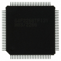
DF2266TF13V Renesas Electronics America, DF2266TF13V Datasheet - Page 540

DF2266TF13V
Manufacturer Part Number
DF2266TF13V
Description
IC H8S/2266 MCU FLASH 100-TQFP
Manufacturer
Renesas Electronics America
Series
H8® H8S/2200r
Datasheet
1.DF2266TF20V.pdf
(712 pages)
Specifications of DF2266TF13V
Core Processor
H8S/2000
Core Size
16-Bit
Speed
13MHz
Connectivity
I²C, SCI, SmartCard
Peripherals
LCD, POR, PWM, WDT
Number Of I /o
67
Program Memory Size
128KB (128K x 8)
Program Memory Type
FLASH
Ram Size
8K x 8
Voltage - Supply (vcc/vdd)
3 V ~ 5.5 V
Data Converters
A/D 10x10b
Oscillator Type
Internal
Operating Temperature
-20°C ~ 75°C
Package / Case
100-TQFP, 100-VQFP
Lead Free Status / RoHS Status
Lead free / RoHS Compliant
Eeprom Size
-
- Current page: 540 of 712
- Download datasheet (5Mb)
Section 17 LCD Controller/Driver
Table 17.6 Output Levels
17.4.3
The H8S/2268 Group incorporates a triple step-up voltage circuit. Triple voltage of liquid crystal
input reference voltage (V
Before enabling the step-up voltage circuit, duty cycle (1/3 duty or 1/4 duty), LCD driver or I/O
pin function, and display data and frame frequency should be selected. Around 0.1-µF capacitor
should be connected between C1 and C2, and voltage specified in section 25.2.6, LCD
Characteristics should be applied to V3 pin.
After above settings, by selecting the step-up voltage circuit clock in LCD control register 2
(LCR2) and setting SUPS to 1, the triple step-up voltage circuit operates, voltage double of V
is generated for V2 pin, and voltage triple of V
Notes: 1. The triple step-up voltage circuit should only be used as LCD drive power of the
Rev. 5.00 Sep. 01, 2009 Page 488 of 656
REJ09B0071-0500
Data
M
Static
1/2 duty
1/3 duty
1/4 duty
2. When the triple step-up voltage circuit is used, do not specify static or 1/2 duty as duty
3. Do not use capacitance with polarity such as electrolytic capacitor as capacitance to be
Triple Step-Up Voltage Circuit (Supported Only by the H8S/2268 Group)
H8S/2268 Group. To drive large panel, power supply capacitance may be insufficient.
In this case, Vcc should be used as power supply or external power supply circuit
should be used.
cycle.
connected between C1 and C2.
Common output
Segment output
Common output
Segment output
Common output
Segment output
Common output
Segment output
LCD3
) input from V3 pin can be used for the LCD driver.
0
0
V1
V1
V2, V3
V1
V3
V2
V3
V2
LCD3
is generated for V1pin.
0
1
V
V
V2, V3
V
V2
V3
V2
V3
SS
SS
SS
1
0
V1
V
V1
V
V1
V
V1
V
SS
SS
SS
SS
1
1
V
V1
V
V1
V
V1
V
V1
SS
SS
SS
SS
LCD3
Related parts for DF2266TF13V
Image
Part Number
Description
Manufacturer
Datasheet
Request
R

Part Number:
Description:
CONN SOCKET 2POS 7.92MM WHITE
Manufacturer:
Hirose Electric Co Ltd
Datasheet:

Part Number:
Description:
CONN SOCKET 4POS 7.92MM WHITE
Manufacturer:
Hirose Electric Co Ltd
Datasheet:

Part Number:
Description:
CONN SOCKET 5POS 7.92MM WHITE
Manufacturer:
Hirose Electric Co Ltd
Datasheet:

Part Number:
Description:
CONN SOCKET 3POS 7.92MM WHITE
Manufacturer:
Hirose Electric Co Ltd
Datasheet:

Part Number:
Description:
CONN SOCKET 5POS 7.92MM WHITE
Manufacturer:
Hirose Electric Co Ltd
Datasheet:

Part Number:
Description:
CONN SOCKET 2POS 7.92MM WHITE
Manufacturer:
Hirose Electric Co Ltd
Datasheet:

Part Number:
Description:
CONN SOCKET 3POS 7.92MM WHITE
Manufacturer:
Hirose Electric Co Ltd
Datasheet:

Part Number:
Description:
CONN SOCKET 4POS 7.92MM WHITE
Manufacturer:
Hirose Electric Co Ltd
Datasheet:

Part Number:
Description:
CONN HEADER 2POS 7.92MM R/A TIN
Manufacturer:
Hirose Electric Co Ltd
Datasheet:

Part Number:
Description:
CONN HEADER 4POS 7.92MM R/A TIN
Manufacturer:
Hirose Electric Co Ltd
Datasheet:

Part Number:
Description:
KIT STARTER FOR M16C/29
Manufacturer:
Renesas Electronics America
Datasheet:

Part Number:
Description:
KIT STARTER FOR R8C/2D
Manufacturer:
Renesas Electronics America
Datasheet:

Part Number:
Description:
R0K33062P STARTER KIT
Manufacturer:
Renesas Electronics America
Datasheet:

Part Number:
Description:
KIT STARTER FOR R8C/23 E8A
Manufacturer:
Renesas Electronics America
Datasheet:

Part Number:
Description:
KIT STARTER FOR R8C/25
Manufacturer:
Renesas Electronics America
Datasheet:


