EVB9311 SMSC, EVB9311 Datasheet - Page 193
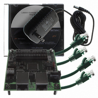
EVB9311
Manufacturer Part Number
EVB9311
Description
EVALUATION BOARD LAN9311-NU
Manufacturer
SMSC
Series
0133r
Datasheet
1.LAN9311-NU.pdf
(460 pages)
Specifications of EVB9311
Main Purpose
Interface, Ethernet
Embedded
No
Utilized Ic / Part
LAN9311
Primary Attributes
2 Ports, 100BASE-TX/10BASE-T, Managed
Secondary Attributes
2 PHYs with HP Auto-MDIX, Auto- Flow Control, 32-bit CRC, MDI/MDI-X
Lead Free Status / RoHS Status
Lead free / RoHS Compliant
Other names
638-1076


Two Port 10/100 Managed Ethernet Switch with 16-Bit Non-PCI CPU Interface
Datasheet
SMSC LAN9311/LAN9311i
14.2.3
14.2.3.1
31:30
29:28
27:16
15:14
BITS
13
12
RESERVED
GPIO 1588 Timer Interrupt Clear Enable 9-8
(GPIO_1588_TIMER_INT_CLEAR_EN[9:8])
These bits enable inputs on GPIO9 and GPIO8 to clear the
1588_TIMER_INT bit of the
(1588_INT_STS_EN). The polarity of these inputs is determined by
GPIO_INT_POL[9:8].
Note:
GPIO Interrupt Polarity 11-0 (GPIO_INT_POL[11:0])
These bits set the interrupt polarity of the 12 GPIO pins. The configured
level (high/low) will set the corresponding GPIO_INT bit in the
Purpose I/O Interrupt Status and Enable Register
0: Sets low logic level trigger on corresponding GPIO pin
1: Sets high logic level trigger on corresponding GPIO pin
GPIO_INT_POL[9:8] also determines the polarity of the GPIO IEEE 1588
time clock capture events and the GPIO 1588 Timer Interrupt Clear inputs.
Refer to
information.
1588 GPIO Output Enable 9-8 (1588_GPIO_OE[9:8])
These bits configure GPIO 9 and GPIO 8 to output 1588 clock compare
events.
0: Disables the output of 1588 clock compare events
1: Enables the output of 1588 clock compare events
Note:
GPIO 9 Clock Event Polarity (GPIO_EVENT_POL_9)
This bit determines if the 1588 clock event output on GPIO 9 is active high
or low.
0: 1588 clock event output active low
1: 1588 clock event output active high
GPIO 8 Clock Event Polarity (GPIO_EVENT_POL_8)
This bit determines if the 1588 clock event output on GPIO 8 is active high
or low.
0: 1588 clock event output active low
1: 1588 clock event output active high
GPIO/LED
This section details the General Purpose I/O (GPIO) and LED related System CSR’s.
General Purpose I/O Configuration Register (GPIO_CFG)
This read/write register configures the GPIO input and output pins. The polarity of the 12 GPIO pins
is configured here as well as the IEEE 1588 timestamping and clock compare event output properties
of the GPIO[9:8] pins.
Section 13.2, "GPIO Operation," on page 163
The GPIO must be configured as an input for this function to
operate. For the clear function, GPIO inputs are edge sensitive and
must be active for greater than 40 nS to be recognized.
These bits override the direction bits in the
Data & Direction Register (GPIO_DATA_DIR)
the GPIO buffer type (GPIOBUF[11:0]) in the
Configuration Register (GPIO_CFG)
Offset:
1588 Interrupt Status and Enable Register
1E0h
DESCRIPTION
DATASHEET
193
is not overridden.
Size:
(GPIO_INT_STS_EN).
General Purpose I/O
General Purpose I/O
register. However,
for additional
General
32 bits
TYPE
R/W
R/W
R/W
R/W
R/W
RO
Revision 1.7 (06-29-10)
DEFAULT
00b
0h
0h
1b
1b
-
Related parts for EVB9311
Image
Part Number
Description
Manufacturer
Datasheet
Request
R


Part Number:
Description:
FAST ETHERNET PHYSICAL LAYER DEVICE
Manufacturer:
SMSC Corporation
Datasheet:
Part Number:
Description:
357-036-542-201 CARDEDGE 36POS DL .156 BLK LOPRO
Manufacturer:
SMSC Corporation
Datasheet:
Part Number:
Description:
357-036-542-201 CARDEDGE 36POS DL .156 BLK LOPRO
Manufacturer:
SMSC Corporation
Datasheet:
Part Number:
Description:
357-036-542-201 CARDEDGE 36POS DL .156 BLK LOPRO
Manufacturer:
SMSC Corporation
Datasheet:
Part Number:
Description:
4-PORT USB2.0 HUB CONTROLLER
Manufacturer:
SMSC Corporation
Datasheet:
Part Number:
Description:
Manufacturer:
SMSC Corporation
Datasheet:
Part Number:
Description:
Manufacturer:
SMSC Corporation
Datasheet:
Part Number:
Description:
FDC37C672ENHANCED SUPER I/O CONTROLLER WITH FAST IR
Manufacturer:
SMSC Corporation
Datasheet:
Part Number:
Description:
COM90C66LJPARCNET Controller/Transceiver with AT Interface and On-Chip RAM
Manufacturer:
SMSC Corporation
Datasheet:
Part Number:
Description:
Manufacturer:
SMSC Corporation
Datasheet:
Part Number:
Description:
Manufacturer:
SMSC Corporation
Datasheet:
Part Number:
Description:
Manufacturer:
SMSC Corporation
Datasheet:
Part Number:
Description:
Manufacturer:
SMSC Corporation
Datasheet: