EVB9311 SMSC, EVB9311 Datasheet - Page 163
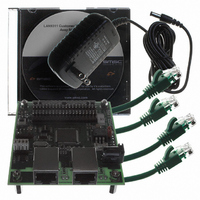
EVB9311
Manufacturer Part Number
EVB9311
Description
EVALUATION BOARD LAN9311-NU
Manufacturer
SMSC
Series
0133r
Datasheet
1.LAN9311-NU.pdf
(460 pages)
Specifications of EVB9311
Main Purpose
Interface, Ethernet
Embedded
No
Utilized Ic / Part
LAN9311
Primary Attributes
2 Ports, 100BASE-TX/10BASE-T, Managed
Secondary Attributes
2 PHYs with HP Auto-MDIX, Auto- Flow Control, 32-bit CRC, MDI/MDI-X
Lead Free Status / RoHS Status
Lead free / RoHS Compliant
Other names
638-1076


Two Port 10/100 Managed Ethernet Switch with 16-Bit Non-PCI CPU Interface
Datasheet
Chapter 13 GPIO/LED Controller
SMSC LAN9311/LAN9311i
13.1
13.2
The GPIO/LED Controller provides 12 configurable general purpose input/output pins, GPIO[11:0].
These pins can be individually configured to function as inputs, push-pull outputs, or open drain outputs
and each is capable of interrupt generation with configurable polarity. Two of the GPIO pins (GPIO[9:8])
can be used for IEEE 1588 timestamp functions, allowing GPIO driven 1588 time clock capture when
configured as an input, or GPIO output generation based on an IEEE 1588 clock target compare event.
In addition, 8 of the GPIO pins can be alternatively configured as LED outputs. These pins, GPIO[7:0]
(nP1LED[3:0] and nP2LED[3:0]), may be enabled to drive Ethernet status LEDs for external indication
of various attributes of the switch ports.
GPIO and LED functionality is configured via the GPIO/LED System Control and Status Registers
(CSRs), accessible through the Host Bus Interface (HBI). These registers are defined in
14.2.3, "GPIO/LED," on page
The GPIO controller is comprised of 12 programmable input/output pins. These pins are individually
configurable via the GPIO CSRs. On application of a chip-level reset:
Note: GPIO[7:0] may be configured as LED outputs by default, dependant on the LED_en_stap[7:0]
The direction and buffer type of all 12 GPIOs are configured via the
Register (GPIO_CFG)
direction of each GPIO, input or output, should be configured first via its respective GPIO direction bit
(GPDIR[11:0]) in the
configured as an output, the output buffer type for each GPIO is selected by the GPIOBUF[11:0] bits
in the
buffers are supported for each GPIO. When functioning as an open-drain driver, the GPIO output pin
is driven low when the corresponding data register bit (GPIOD in the
Direction Register
When a GPIO is enabled as an output, the value output to the GPIO pin is set via the corresponding
GPIOD[11:0] bit in the
configured as inputs, the corresponding GPIOD[11:0] bit reflects the current state of the GPIO input.
Note: For GPIO[9:8], the pin direction is a function of both the GPDIR[9:8] bits of the
Functional Overview
GPIO Operation
All GPIOs are set as inputs (GPDIR[11:0] cleared in
(GPIO_DATA_DIR))
All GPIO interrupts are disabled (GPIO[11:0]_INT_EN cleared in
Status and Enable Register (GPIO_INT_STS_EN)
All GPIO interrupts are configured to low logic level triggering (GPIO_INT_POL[11:0] cleared in
General Purpose I/O Configuration Register
General Purpose I/O Configuration Register
configuration straps. Refer to
Purpose I/O Data & Direction Register (GPIO_DATA_DIR)
the
General Purpose I/O Configuration Register
(GPIO_DATA_DIR)) is cleared to 0, and is not driven when set to 1.
General Purpose I/O Data & Direction Register
General Purpose I/O Data & Direction Register
and
General Purpose I/O Data & Direction Register
193.
DATASHEET
Section 13.3, "LED Operation"
163
(GPIO_CFG))
(GPIO_CFG). Push/pull and open-drain output
General Purpose I/O Data & Direction Register
(GPIO_CFG).
and the 1588_GPIO_OE[9:8] bits in
General Purpose I/O Configuration
General Purpose I/O Interrupt
for additional information.
(GPIO_DATA_DIR). For GPIOs
General Purpose I/O Data &
(GPIO_DATA_DIR). When
(GPIO_DATA_DIR). The
Revision 1.7 (06-29-10)
General
Section
Related parts for EVB9311
Image
Part Number
Description
Manufacturer
Datasheet
Request
R


Part Number:
Description:
FAST ETHERNET PHYSICAL LAYER DEVICE
Manufacturer:
SMSC Corporation
Datasheet:
Part Number:
Description:
357-036-542-201 CARDEDGE 36POS DL .156 BLK LOPRO
Manufacturer:
SMSC Corporation
Datasheet:
Part Number:
Description:
357-036-542-201 CARDEDGE 36POS DL .156 BLK LOPRO
Manufacturer:
SMSC Corporation
Datasheet:
Part Number:
Description:
357-036-542-201 CARDEDGE 36POS DL .156 BLK LOPRO
Manufacturer:
SMSC Corporation
Datasheet:
Part Number:
Description:
4-PORT USB2.0 HUB CONTROLLER
Manufacturer:
SMSC Corporation
Datasheet:
Part Number:
Description:
Manufacturer:
SMSC Corporation
Datasheet:
Part Number:
Description:
Manufacturer:
SMSC Corporation
Datasheet:
Part Number:
Description:
FDC37C672ENHANCED SUPER I/O CONTROLLER WITH FAST IR
Manufacturer:
SMSC Corporation
Datasheet:
Part Number:
Description:
COM90C66LJPARCNET Controller/Transceiver with AT Interface and On-Chip RAM
Manufacturer:
SMSC Corporation
Datasheet:
Part Number:
Description:
Manufacturer:
SMSC Corporation
Datasheet:
Part Number:
Description:
Manufacturer:
SMSC Corporation
Datasheet:
Part Number:
Description:
Manufacturer:
SMSC Corporation
Datasheet:
Part Number:
Description:
Manufacturer:
SMSC Corporation
Datasheet: